Module 2.1
The Hartley Oscillator
- After Studying this section, you should be able to:
- • Understand the operation of The Tuned Tank Circuit.
- • Understand the operation of Automatic (Sliding) Class C Bias.
- • Understand the operation of Hartley Oscillators.
- • Recognise Alternative Hartley Designs.
The Hartley Oscillator
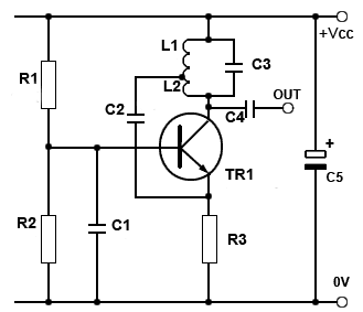
Fig. 2.1.1 The Hartley Oscillator
The Hartley Oscillator is a particularly useful circuit for producing good quality sine wave signals in the RF range, (30kHz to 30MHz) although at the higher limits of this range and above, The Colpitts oscillator is usually preferred. Although both these oscillators oscillator use an LC tuned (tank) circuit to control the oscillator frequency, The Hartley design can be recognised by its use of a tapped inductor (L1 and L2 in Fig. 2.1.1).
The frequency of oscillation can be calculated in the same way as any parallel resonant circuit, using:

Where L = L1 + L2
This basic formula is adequate where the mutual inductance between L1 and L2 is negligible, but needs to be modified when the mutual inductance between L1 and L2 is considerable.
Mutual Inductance in Hartley Oscillators
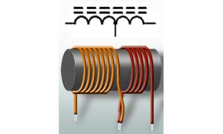
Fig. 2.1.2 Centre Tapped Inductors on a Common Core
Mutual inductance is an additional effective amount of inductance caused by the magnetic field created around one inductor (or one part of a tapped inductor) inducing a current into the other inductor. When both inductors are wound on a common core, as shown in Fig. 2.1.2 the effect of mutual inductance (M) can be considerable and the total inductance is calculated by the formula:
LTOT =L1 + L2 ±2M
The actual value of M depends on how effectively the two inductors are magnetically coupled, which among other factors depends on the spacing between the inductors, the number of turns on each inductor, the dimensions of each coil and the material of the common core.
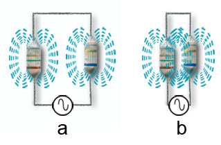
Fig. 2.1.3 Inductors with Adding Fields
With separate fixed inductors, as shown in Fig. 2.1.3a considerations of mutual inductance are simplified, the dimensions and number of turns for each inductor are fixed, therefore main considerations are the physical distance between the inductors and the direction of their magnetic fields. In practice the small values of inductance of the inductors needed at RF create very little magnetic field outside the component, and only when mounted within a couple of millimetres of each other is the mutual inductance effect noticeable, as shown in Fig. 2.1.3b.
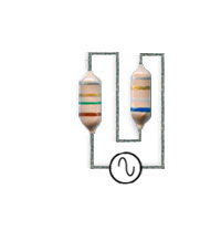
Fig. 2.1.4 Inductors with Opposing Fields
Whether M, measured in Henrys or more likely micro Henrys (µH) in RF oscillators adds to or subtracts from the total inductance of very closely mounted tapped inductors depends on the North-South polarity of the fields around the individual coils L1 and L2, if the magnetic fields are both in the same direction, the mutual inductance will add to the total inductance but if the magnetic fields are arranged to oppose each other, as in Fig.2.1.4 the effect of the mutual inductance will be to reduce the total inductance and so increase the actual working frequency of the oscillator.
The amount of mutual inductance in a circuit using two small fixed inductors such as the circuit featured in Oscillators module 2.2 is minimal, and experiments show that the inductors need to be virtually touching to produce any noticeable effect. Whether the mutual inductance between small inductors of just a few micro Henrys add or subtract from the calculated oscillator frequency of a RF Hartley oscillator, this will generally only change the operating frequency by an amount similar to that which may be caused by the normal component value variation due to the tolerances of the oscillator components.
In practical Hartley oscillators that use inductors sharing a common core however, the mutual induction effect can be much greater, and depends on the coefficient of coupling (k), which has a value between 1 when the mutual inductance is just about equal to 100% magnetic coupling, and 0 when there is no coupling between the two inductors.
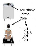
Fig. 2.1.5 Adjustable Ferrite Core
Calculating a theoretical value for k involves some quite complex math due to the number of factors affecting the mutual coupling, and the process is often reduced to deciding whether there is little mutual coupling, so that less than half of the magnetic flux produced by one coil affects the other coil. If so, then k is assumed to have a value less than 0.5, and the inductors are said to be ‘loosely coupled’. Alternatively, if the inductors sharing a common core have zero spacing between them, they are said to be ‘tightly coupled’ and k is assumed to have a value between 0.5 and 1. In practice the core shared by such a tapped inductor working at RF frequencies will often be found to be a variable type as shown in Fig. 2.1.5 so that any frequency shift due to mutual inductance can be adjusted for, by changing the position of the core and so correcting the oscillator frequency.
The Hartley Circuit
Fig. 2.1.1 shows a typical Hartley oscillator. The frequency determining resonant tuned circuit is formed by L1/L2 and C3 and is used as the load impedance of the amplifier. This gives the amplifier a high gain only at the resonant frequency (Method 2 in Introduction to Oscillators). This particular version of the Hartley circuit uses a common base amplifier, the base of TR1 being connected directly to 0V (as far as AC the signal is concerned) by C1. In this mode the output voltage waveform at the collector, and the input signal at the emitter are in phase. This ensures that the fraction of the output signal fed back from the tuned circuit collector load to the emitter via the capacitor C2 provides the necessary positive feedback.
C2 also forms a long time constant with the emitter resistor R3 to provide an average DC voltage level proportional to the amplitude of the feedback signal at the emitter of Tr1. This is used to automatically control the gain of the amplifier to give the necessary closed loop gain of 1.
The emitter resistor R3 is not decoupled because the emitter terminal is used as the amplifier input. The base being connected to ground via C1, which will have a very low reactance at the oscillator frequency.
The Tuned LC (Tank) Circuit
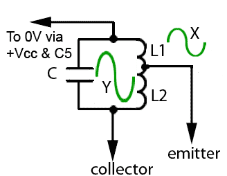
Fig. 2.1.6 The Tank Circuit
The LC circuit that controls the frequency of oscillation is often called the "TANK CIRCUIT" because it contains circulating currents much greater than the current supplying it (e.g. pulses of collector current supplied by the amplifier). Its operation is supposed to be rather like a water tank or cistern that can supply a continuous flow of water from an intermittently flowing external supply. The tank circuit in the oscillator contains high values of circulating current topped up regularly by smaller amounts of current from the amplifier.
Because most of the current flowing in the oscillator is flowing just around the resonant tank circuit rather than though the amplifier section of the oscillator, LC oscillators generally produce a sine wave with very little amplifier sourced distortion.
Another feature of the tank circuit is to provide the correct amount of positive feedback to keep the oscillator running. This is done by dividing the inductive branch of the circuit into two sections, each having a different value, the inductor therefore works in a similar manner to an autotransformer, the ratio of the two windings providing the appropriate amount of signal to be fed back to the input of the amplifier.
Because in Fig. 2.1.6 (and Fig. 2.1.1) the top of L1 is connected to +Vcc, it is, as far as AC signals are concerned, connected to ground via the very low impedance of C5. Therefore waveform X across L1, and waveform Y across the whole circuit are in phase. As a common base amplifier is being used, the collector and emitter signals are also in phase, and the tank circuit is therefore providing positive feedback. In other Hartley designs, using common emitter amplifiers for example, similar tank circuits are used but with different connections, so that the feedback signal is always in phase with the input signal, therefore providing the necessary positive feedback.
Automatic ‘Sliding’ Class C bias
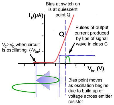
Fig. 2.1.7 Sliding Class C Bias
It is common in LC sine wave oscillators to use automatic class C bias. In class C the bias voltage, that is the base voltage of the transistor is more negative than the emitter voltage, making Vbe negative so that the average (centre) voltage of the input wave is located on the negative portion of the Vbe axis of the characteristic curve shown in Fig. 2.1.7 Therefore only a portion of each sine wave is amplified to produce pulses of collector current.
Because only the tips of the waveform are amplified in class C, the amplifier cannot produce an undistorted output wave. This does not matter however, in an LC oscillator. All the amplifier is required to do is to provide pulses of current to the LC resonant circuit at its resonating frequency. The sine wave output of the circuit is actually produced by the resonating action of the LC circuit. The amplitude of the signal produced will depend on the amount of current flowing in the LC tuned circuit.
As the amplifier provides this current it follows that, by automatically controlling the amount of collector current (Ic) flowing each time a pulse is produced, the amplitude of the output sine wave can be controlled at a constant level. The collector current of the transistor depends on the base/emitter voltage. In class C the base/emitter voltage is automatically varied so that the amplitude of the output wave remains stable.
How the Hartley Oscillator Works
The oscillator in Fig. 2.1.1 uses a common base amplifier. When the oscillator is first powered up, the amplifier is working in class A with positive feedback. The LC tank circuit receives pulses of collector current and begins to resonate at its designed frequency. The current magnification provided by the tank circuit is high, which initially makes the output amplitude very large. However, once the first pulses are present and are fed back to the emitter via C2, a DC voltage, dependent to a large extent on the time constant of C2 and R3, which is much longer than the periodic time of the oscillator wave, builds up across R3.
As the emitter voltage increases, the bias point of the amplifier ‘slides’ from its class A position towards class C conditions, as shown in Fig 2.1.7, reducing the difference (Vbe) between the relatively stable base voltage created by the potential diver Rl/R2 and the increasingly positive emitter voltage. This reduces the portion of the waveform that can be amplified by TR1, until just the tips of the waveform are producing pulses of collector current through the tank circuit and the closed loop gain circuit has reduced to 1. Effectively the positive feedback from the tank circuit and the negative and feedback created by C2 and R3 are in balance.
Any deviation from this balance creates a correcting effect. If the amplitude of the output wave reduces, the feedback via C2 also reduces causing the emitter voltage to decrease, making negative value of Vbe smaller, and so creating a correcting increase in collector current and a greater output wave produced across the tank circuit. As collector current increases, then so will TR1 emitter voltage. This will cause a larger voltage across R3 making the emitter more positive, effectively increasing the amount of negative base/emitter voltage of Tr1. This reduces collector current again, leading to a smaller output waveform being produced by the tank circuit and balancing the closed loop gain of the circuit at 1.
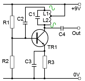
Fig. 2.1.8 Common Emitter Hartley Oscillator
Alternative Hartley Designs.
The circuit shown in Fig. 2.1.8 uses a common emitter amplifier and positive feedback from the top of the tuned circuit, via C2 (DC blocking and AC coupling capacitor) to the base.
The top and bottom ends of the tapped inductor L1/L2 are in anti-phase as in this design, the tapping point of the tank circuit is connected to the supply line, which in a common emitter amplifier it is exactly the same point as the transistor emitter due to the decoupling capacitors across the supply (not shown as they will be in the power supply), and C3 across the emitter resistor.
The base in a common emitter amplifier is also in anti-phase with the collector waveform, resulting in positive feedback via C2. Automatic class C bias is again used but in this circuit the value of the emitter decoupling capacitor C3 will be critical, and smaller than in a normal class A amplifier. It will only partially decouple R3, the time constant of R3/C3 controlling the amount of class C bias applied.
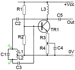
Fig. 2.1.9 Hartley Oscillator with Tuned Feedback
In Fig. 2.1.9 the tapping on the inductor is connected to ground rather than +Vcc, and two DC blocking capacitors are used to eliminate any DC from the tuned circuit. The collector load is now provided by a RF choke which simply provides a high impedance at the oscillator frequency.
Automatic class C bias is provided for the common emitter amplifier in a similar manner to Fig. 2.1.8. In this variation however, rather than using a tuned amplifier that amplifies only at the desired frequency, the amplifier here will operate over a wide range of frequencies.
However placing the tuned tank circuit in the feedback path ensures that positive feedback only occurs at the resonant frequency of the tuned circuit.


