Module 4.3
555 Astables
- After Studying this section, you should be able to:
- • Understand the basic operation of a 555 timer.
- • Understand the operation of a 555 timer in astable mode.
- • Understand time constants in a 555 timer.
- • Calculate the frequency of a 555 timer in astable mode.
Astable Oscillators Using the 555 Timer
A popular way of implementing an astable square wave oscillator is to use the 555 Timer IC. This is one of the most commonly available Timer ICs and has many different uses. As well as being used to construct astable oscillators, it can also be used in monostable mode where an input pulse is used to trigger a time delay set by an RC time constant, during which the output pin goes to a high level (+Vcc) and then returns to 0V to await a further trigger pulse at the IC input pin.
The 555 Timer IC

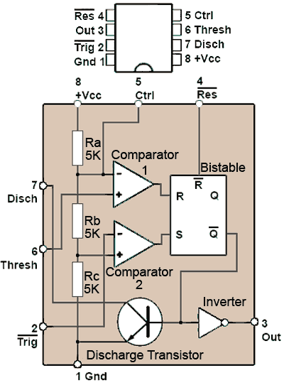
Fig. 4.3.1 The 555 Timer IC
The 555 in its astable configuration can be used to generate a square wave signal with a number of variations:
- • Square wave with even or uneven mark to space ratio
- • Pulse train
- • Pulse width modulation
- • Pulse position modulation
- • Frequency modulation
The internal component parts of the 555 Timer IC together with the IC pin out are illustrated in Fig. 4.3.1, the function of the pins are as follows:
Pin 1. Gnd = Ground connection.
Pin 2. Trig = Trigger (active low).
This active low pin (indicated by the horizontal bar above its name) is normally high (at +Vcc) but when it is momentarily taken low (below 1/3 Vcc) it initiates a sequence of internal events that make the output (pin 3) go high for a period of time set by the value of an external RC time constant.
Pin 3. Out = Output.
The output goes high (to +Vcc) during a time constant period then returns to 0V. When the IC is operated in astable mode two time constants are involved, one governing the high, and one the low condition. The output is capable of sinking and sourcing up to 200mA, which makes it capable of driving a number of commonly used devices such as LEDs, relays, lamps and small motors without the need for external driver stages.
Pin 4. Res = Reset (active low).
Normally high but when taken low makes the Q output of the internal bi-stable to reset to its low state, and Q (the inverse of Q) goes to its high state. This immediately makes the output (pin 3) 0V and also causes the Discharge transistor to discharge the external time constant capacitor. If the Reset pin is taken high again the output stays in its reset (0V) condition until the IC is triggered once more by an input trigger pulse at pin 2. In circuits where reset is not required it is normally connected directly to +Vcc. The reset pin can also be used as an ‘Inhibit’ control. For example it can be used to prevent the action of an astable oscillator driving a buzzer, until such time as its signal is needed.
Pin 5. Ctrl = Control.
Pin 5 allows for the application of a variable voltage to control the length of time of the RC time constant, and so can be used to vary the frequency and/or the mark to space ratio used in generating the output wave. The higher the voltage on the control pin, the longer the periodic time and the lower the frequency of the astable. This enables the IC to be used for such purposes as frequency modulation, by altering the frequency generated by the 555 in astable mode in response to a changing voltage or low frequency signal applied to the control pin.
With an astable producing an uneven mark to space ratio (i.e. pulses) the control pin can also be used to vary the mark to space ratio and so produce pulse width modulation (PWM). Alternatively, if the output of the 555 in astable mode is a series of very narrow negative going pulses, then applying a modulating signal to the control input can be made to vary the high period between the pulses, effectively producing pulse position modulation.
The control pin can also be used with the 555 in monostable mode to vary the time of the generated delay. When the control pin is not being used for timing control, it is not connected to any external voltage, so to prevent any external noise from entering pin 5 it is decoupled, typically using a capacitor of around 100nF .
As pin 5 is connected internally to the junction between Ra and Rb, the voltage on pin 5 when not in active use will be 2/3Vcc.
Pin 6. Thresh = Threshold
In astable mode pin 6 is connected externally to the RC time constant charging capacitor, and so as the capacitor charges, the voltage on pin 6 increases. This causes the voltage on the non-inverting input to Comparator 1, to rise until it reaches the threshold level of 2/3Vcc set by the inverting input of Comparator 1 being connected to the junction between Ra and Rb. Once the voltage on pin 6 reaches 2/3Vcc, Comparator 1 output suddenly changes state and initiates a sequence of events that causes the external time constant capacitor to begin discharging.
Pin 7. Disch = Discharge
Pin 7 is connected to the collector of the discharge transistor, and once the threshold pin has tripped Comparator 1 at the end of the charging period for the external timing capacitor, the discharge transistor conducts, causing the discharge period to commence. During this period the output (pin 3) will be held low until the capacitor has discharged to 1/3Vcc when, in astable mode, the Discharge Transistor will turn off and the charging period will start again. In monostable mode however, the capacitor will be discharged completely to 0V to await another trigger pulse at pin 2.
Pin 8. +Vcc = Positive supply voltage
The 555 is available in a number of variant forms including BJT and CMOS types. Depending on type they can operate from positive supplies ranging from 0.9V to 18V with a current requirement ranging from less than 50μA to 10mA for the chip itself. This current requirement must be added to the current needs of any output device, which will be supplied by the output of the 555 when it is in high mode. This load current can be anything up to 200mA depending on the load.
The 555 Astable Oscillator

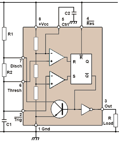
Fig. 4.3.2 The 555 Astable
As shown in Fig 4.3.2 a basic astable requires only two resistors and two capacitors (not including the external load).
The RC time constant that determines the pulse width and frequency is made up of C1 R1 and R2. Pins 6 and 2 are connected together, pin 4 is connected directly to supply as reset is not being used, and the control input on pin 3 is decoupled with a 100nF capacitor.
To produce a square wave output, with a mark to space ratio approaching 1:1, R2 should be a much higher value than R1. The reason for this is in the way that the 555 works.
Astable operation
When power is initially applied to pin 8, capacitor C1 has no charge and so pin 2, the trigger input is active at 0V and C1 begins to charge towards the supply voltage (Vcc) via R1 and R2. As C1 is also connected to pin 6, the voltage on the non-inverting (+) input of comparator 1 also increases. In this condition the output (pin3) will be at Vcc and able to act as a source of current to any load, of up to 200mA.
The inverting (-) input of comparator 1 is connected to the resistor chain Ra, Rb and Rc, which are connected between Vcc and 0V. Since all three resistors have the same value (5K) the voltage on the inverting input will be 2/3Vcc.
So long as the voltage on the non-inverting input of comparator 1 is lower than that on its inverting input, its output will be low (at approximately 0V), but as soon as C1 charges up to 2/3Vcc the comparator will change to its high level (Vcc). This puts a high level on the R (Reset) input of the bistable.
When the R input of the bistable goes high the Q output is reset to zero, and as the (not Q) output is always in the opposite state to the Q output, ‘not Q’ goes high. This has the effect of causing the discharge transistor to conduct heavily, connecting the Discharge pin (7) virtually to ground, so discharging the capacitor C1 via R2. The high voltage on the output of the bistable is also fed to the inverter, which changes this level to a ‘low’ of approximately 0V at the output.
The output of the inverter now allows the output to ‘sink’ up to 200mA.
Once the C1 begins to discharge however, the output of comparator 1 will return to a low level, but this doesn’t matter as the bi-stable will ‘remember’ the very short high pulse delivered to its R input by comparator 1 and will remain in its ‘reset’ state until it receives a similar ‘set’ pulse at its S input.
Notice that when C1 charged, it did so via both R1 and R2, but it now discharges through R2 only. It is for this reason that R1 is made much smaller than R2. If both resistors were equal in value the discharge time (when the output is low) would be half the charge time (when the output is high). By having a ratio of about 100:1 for the values of R2:R1 the mark to space ratio can be made very nearly (but not quite) 1:1.
The falling voltage across C1 is connected to the non-inverting (+) input of comparator 2 so once this voltage falls below that on the inverting (-) input, which it will do at a level of 1/3Vcc, as the inverting input is fed from the top of the lowest resistor Rc in the potential divider resistance chain, the output of comparator 2 will go to its high (Vcc) level. This is fed to the S input of the bi-stable causing the Q and Q output to swap their high and low states, making the output low once more, switching off the discharge transistor and, via the inverter, making the output (pin 3) high.

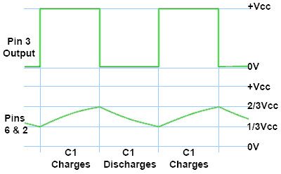
Fig. 4.3.3 Astable Output & Charging Waveforms

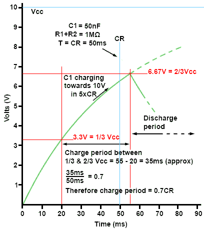
Fig. 4.3.4 The Charge Period of C1
That completes one whole cycle of the output square wave, and C1 now begins to charge once more towards 2/3Vcc and the cycles repeat as long as power is applied.
Time Constants and the 555
The relationship between the output wave and the charging and discharging of C1 is illustrated in Fig. 4.3.3. The charge time is dependent on the time constant (R1 +R2)C1 and the discharge time is dependent on the time constant R2C1 so the discharge time will always be shorter than the charge time. However when R2 is much greater than R1 the charge and discharge times are nearly equal, and for the purpose of calculating the frequency of oscillation R1 may be ignored, so the period of one cycle is simply the two periods added together.
There is another complication however, the time of the charge or discharge period is not simply the time constant CR because the capacitor is not being allowed to fully charge or discharge, only the central 1/3 of the full charge or discharge is being used, so in calculating the periodic time of the waveform, a constant must be used to modify the normal T = CR time constant formula.
Fig. 4.3.4 illustrates how the time constant formula is modified to make it suitable for calculating the periodic times relating specifically to the 555 astable.
In this example C1 is 50nF and it charges via R1 and R2, which have a combined series resistance of 1MΩ. Therefore the normaltime constant (T = CR) is 50ms and with a supply voltage (Vcc) of 10V, C1 will charge to 3.3V (1/3Vcc) in 20ms and reach 6.67V (2/3Vcc) after 55ms (35ms later).
The voltage across C1 would continue to rise to 10V after 5 time constants, except that at 2/3Vcc comparator 1 will switch on (see Fig. 4.3.3) and C1 will begin its discharge period. C1 has therefore charged for only thirty five fiftieths (35/50) or 0.7 of the time constant.
Calculating the Frequency of a 555 Astable
The charge period as C1 charges via R1 andR2 may be calculated as:
Charge (high output) period:
(tC) = 0.7x(R1+R2)xC1
Because R1 does not play a part in the discharge period this would be calculated as:
Discharge (low output) period:
tD = 0.7xR2xC1
The periodic time of the whole wave (T) will therefore be:
T = Charge period tC + Discharge period tD
so
T = (0.7x(R1+R2)xC1) + (0.7xR2xC1)
Therefore
T =0.7 (R1+2R2) C1
As frequency (f)= 1/T the formula for the frequency of a 555 astable can be written as:

And as 1/0.7 = 1.4 the formula for the frequency of a 555 astable can also be written as:


