Google Ads
Module 8.2
How Filters Work
- After studying this section, you should be able to describe:
- How passive filters achieve frequency selective attenuation and phase change with reference to phasor diagrams.
- • High pass filters.
- • Low pass filters.
CR Filter Operation.
Figs 8.2.1 and 8.2.2 show two common methods of using C and R together to achieve alterations in AC signals. These CR combinations are used for many purposes in a wide variety of circuits. This section describes their effects when used as filters with sine wave signals of varying frequencies such as simple tone or Bass/Treble controls in audio circuts. Similar CR combinations are also used to change the shape of non-sinusoidal waves. Such waves as square waves contain many harmonics of differnt frequencies and by reducing the amplitude of some of these harmonics, the wave shape is changed. The techniques used for this purpose are described in Differentiators and Integrators later in this this module.
The High Pass CR Filter

Fig 8.2.1 High Pass CR Filter
The CR circuit illustrated in Fig 8.2.1, when used with sinusoidal signals is called the HIGH PASS FILTER. Its purpose is to allow high frequency sine waves to pass unhindered from its input to its output, but to reduce the amplitude of, (to attenuate) lower frequency signals. A typical application of this circuit would be the correction of frequency response (tone correction) in an audio amplifier.
As described in Module 6, resistance is constant at any frequency, but the opposition to current flow offered by the capacitor (C) however, is due to capacitive reactance XC, which is greater at low frequencies than at high frequencies.
The reactance of the capacitor (XC) and the resistance of the resistor (R) in fig 8.2.1 act as a potential divider placed across the input, with the output signal taken from the centre of the two components. At low frequencies where XC is much greater than R, the share of the signal voltage across R will be less than that across C and so the output will be attenuated. At higher frequencies, it is arranged, by suitable choice of component values, that the resistance of R will be much greater than the (now low) reactance XC, so the majority of the signal is developed across R, and little or no attenuation will occur.
The Low Pass CR Filter

Fig 8.2.2 Low Pass CR Filter
In Fig 8.2.2 the positions of the resistor and capacitor are reversed, so that at low frequencies the high reactance offered by the capacitor allows all, or almost all of the input signal to be developed as an output voltage across XC. At higher frequencies however, XC becomes much less than R and little of the input signal is now developed across XC. The circuit therefore attenuates the higher frequencies applied to the input and acts as a LOW PASS FILTER.
The band of frequencies attenuated by high and low pass filters depends on the values of the components. The frequency at which attenuation begins or ends can be selected by suitable component choices. In cases of audio tone correction, the resistor may be made variable, allowing a variable amount of bass or treble (low or high frequency) cut. This is the basis of most inexpensive tone controls
High and low pass filters can also be constructed from L and R. In this case the action is the same as for the CR circuit except that the action of XL is the reverse of XC. Therefore in LR filters the position of the components is reversed.
Phase Change in Filters
The above description of high and low pass filters explains how they operate in terms of resistance and reactance. It shows how gain (Vout/Vin) is different at high and low frequencies due to the relative values of XC and R. However this simple explanation does not take the phase relationships between capacitors or inductors, and resistors into account. To accurately calculate voltage values across the components of a filter it is necessary to take phase angles into consideration as well as resistance and reactance. This can be done by using phasor diagrams to calculate the values graphically, or by a branch of algebra using ´complex numbers´ and ´j Notation´. However these calculations can also be done using little more than the Reactance calculations learned in Module 6 and the Impedance Triangle calculations from Module 7.
Problem:
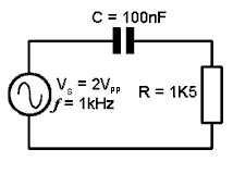
Calculate the peak to peak voltages Vr appearing across R and Vc appearing across C when an AC supply voltage of 2Vpp at 1kHz is applied to the circuit as shown.
Although C and R form a potential divider across Vs it is not possible to calculate these values using the potential divider equation(because phase angles must also be taken into account):

Follow these steps:
1. Find the value of capacitive reactance XC using:


2. Use the Impedance Triangle to find Z (the impedance of the whole circuit).


3. Knowing that the supply voltage Vs is developed across Z, the next step is to calculate the volts per ohm (V/Ω),

Because the volts per ohm will be the same for each component as it is for the circuit impedance, the result from step 3 can now be used to find the voltages across C, and across R.


If required, the Phase angle θ could also be found using trigonometry as described in Phasor Calculations, Module 5.4 (Method 3). To find the angle θ (the phase difference between the supply voltage VS and the supply current, which would be in the same phase as VR) the two voltages already found could be used.

Because circuits containing capacitance (or inductance) in addition to resistance affect the phase relationships of sine wave signals. This allows these same circuits to be used to change the PHASE of signals instead of, or as well as the amplitude.
CR Filter Operation
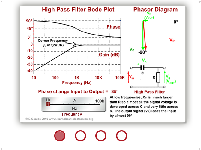
Fig 8.2.3 demonstrates how phasor diagrams can explain both the amplitude and phase effects of a CR filters. Click on the direction arrowheads to see how a high pass filter operates at different frequencies and notice that it is the input voltage (VIN that apparently changes phase, but this is just because the circuit current phasor (and therefore the VR phasor, which is always in phase with the current) is used as the static reference phasor. The thing to remember is that there is a phase change of between 0° and 90° happening between VIN and VOUT, which depends on the frequency of the signal.
Using phasor diagrams to explain the high pass filter shows that:
• In The High pass Filter (Fig. 8.2.3) at low frequencies the output VOUT (VR) is much smaller than VIN (VC) and a phase shift of up to 90° occurs with the output phase leading the input phase.
• At high frequencies there is little or no difference between the relative amplitudes of VOUT (VR) and VIN , and little or no phase shift is taking place. At the corner frequency fc the phase shift is 45° and below that the Bode plot shows that frequency gain falls off at a steady rate of -20dB per decade.
For more information on Bode Plots and how they can be used together with phasor diagrams to illustrate the operation of a low pass filter, see Bode Plots where Fig 8.3.2 similarly demonstrates the action of a CR Low Pass Filter. In this circuit note that VOUT = VC so the output phase lags the input phase by up to about -90°, depending on the input frequency