Google Ads
Module 2.2
Class A Amplifier Design
- After studying this section, you should be able to:
- Design a basic class A common emitter audio amplifier.
- • Calculate capacitor values for coupling and decoupling components.
- • Assemble a prototype amplifier on Breadboard
Part 2. Adding the AC Components.

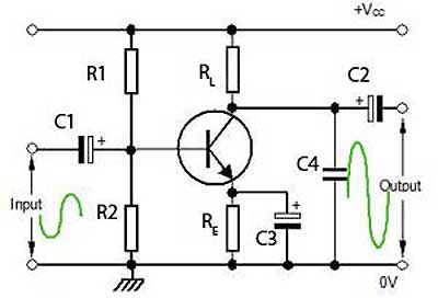
Fig. 2.2.1. Common Emitter Amplifier
Choosing a value for C1 and C2
Calculate the component values and record your results in Part 2 of the Amplifier Design Record sheets.
The primary function of C1 and C2 is to act as coupling capacitors, allowing AC signals to pass whilst blocking DC at the input and output so that voltages present on preceding or later circuits will not upset the bias condition for this amplifier.
The main consideration in choosing these capacitor values is to ensure that their capacitive reactance is low enough, compared with the input impedance of the amplifier, or any load connected to the output, to allow signals at all the required frequencies to pass.
The reactance of a capacitor is greatest at low frequencies, therefore the choice of coupling capacitor values must allow for a low reactance at the lowest frequencies the amplifier is designed to amplify. A generally accepted value for coupling capacitors in an audio amplifier would be between 1µF and 10µF, (this can be changed later when the design is finalised).
Choosing a value for C3
The purpose of C3 is to prevent any AC signal voltage appearing across the emitter resistor RE. Any AC appearing on the emitter of the transistor would be in phase with the signal at the base, therefore the base and emitter voltages would rise and fall together, and the difference between base and emitter voltages would be reduced. This would effectively reduce the input signal and so reduce the amplifier´s gain.
C3 must therefore remove as much of the AC from across RE as possible and so must have a low reactance at all audio frequencies. As the lowest frequency is going to be around 20Hz, C3 must have a reactance (XC) that is small compared to the value of RE at all frequencies above 20Hz .
The value of C4

The purpose of C4 is to give an appropriate reduction in amplification at the high frequency end of the amplifier´s bandwidth. The choice of its value will be covered after initial testing of the amplifier. At this stage it is not necessary to fit C4.
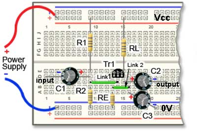
Fig. 2.2.2 Fitting the AC components.
After switching off the power to the circuit, capacitors C1, C2 and C3 can now be added to the circuit on the ´Bread board´ for testing.

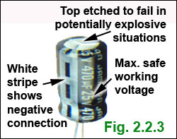
WARNING: Be extra careful when connecting electrolytic capacitors to ensure they are connected with the correct polarity, see Fig. 2.2.3 showing negative lead marking on a capacitor, but note that the convention in circuit schematic diagrams (Fig. 2.2.1) is to mark the positive plate of an electrolytic capacitor with a + symbol. Fig. 2.2.3 also shows the safe working voltage of the capacitor, which must be high enough to withstand any likely voltage the capacitor will be subject to in the circuit.
Connecting electrolytic capacitors the wrong way round, or exceeding their working voltage can cause them to EXPLODE!
Carry out the initial checks in Part 3 before re-connecting the power.


