Module 3.1
Logic Families Compared
- After studying this section, you should be able to:
- Recognise Logic Families.
- • CMOS ,TTL and ECL.
- • Device Identification.
- Understand differences between logic families.
- • Speed and power considerations.
- • Pin compatibility.
Power, Speed and Compatibility
The logic gates (introduced in Module 2.1) are available in different combinations within I/C packages. As well as the basic logic functions, compatible ICs are available, which contain particular useful combinations of gates providing a convenient way of constructing more complex circuits. Hundreds of different, but directly inter-connectable logic ICs are available. The most commonly available logic ICs are the 74 series family and its sub−families, identifiable because their type numbers all start with the number 74.

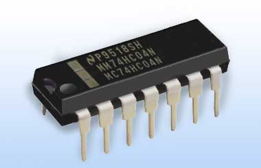
Fig.3.1.1 Logic IC Device Numbering
74 Series Device Identification
A typical 74 series IC is shown in Fig 3.1.1 and can be identified by the number MC74HC04N, which is a common structure for 74 series logic ICs, which breaks down into several sections as follows:
MC − One to three letter manufacturer’s ID code. (e.g. National Semiconductor/Texas Instruments)
74 − Commercial grade, IC plastic package with temperature range of 0°C to +70°C although some sub families have an extended range of − 40°C to +125°C.
(Also 54 Military/Aerospace grade, IC ceramic package with temperature range of −55°C to +125°C).
HC − Two to three letter code indicating sub-family (HC = High speed CMOS, HCT = High speed CMOS, TTL compatible).
04 − Two to four digit type number, indicates the type of circuit or gates with IC. 04 = Hex (6 per IC) Inverters.
N − One or two letter code for package type, e.g. N = DIP - Dual Inline Package. The codes used vary between manufacturers, but package details are usually included on the IC datasheet.
Compatibility between Logic ICs
The use of a single family within a circuit design with direct connections between ICs enables circuit designers to produce circuits consisting mainly of ICs, with few extra coupling or biasing components. This greatly reduces the component count of a circuit, which among other benefits, reduces size and increases reliability.
ICs of a particular family generally use a common technology, but ICs in other families, using different technologies, usually have different input and output requirements, different supply voltages, and other parameters that affect the use of digital ICs. Making direct connections between ICs of a single family or sub family is usually very simple. ICs of different families can sometimes also be directly connected together, but may require some extra circuitry at the interface of the two IC families to maintain compatibility.
Why these different families exist dates back to the 1960s when groups of logic ICs using different technologies first became available.
Scale of Integration

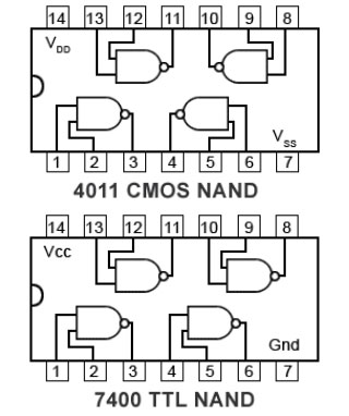
Fig. 3.1.2 Original CMOS and TTL Pinouts for Comparable NAND gate ICs
RTL (resistor-transistor logic) and DTL (diode-transistor logic), successfully used in early computers were superseded by TTL (transistor-transistor logic), which became the dominant technology. However as these ICs developed, at first as SSI (small scale integrated) devices, with just a few transistors per chip, and then as MSI (medium scale integrated) devices with 100 or more transistors, a problem arose that as more gates (and therefore more transistors) were packed into a single IC, the scale of integration would be limited by the power dissipation of the device.
Although each gate only dissipates a few milliWatts, the heat generated within a single large-scale integrated (LSI) circuit containing tens of thousands of transistors could potentially quickly destroy the IC.
It was therefore necessary to develop gates with much lower power consumption, so in the 1970s a series of CMOS (Complimentary Metal Oxide Semiconductor) ICs, called the 4000 series was developed, in which the power consumed by each gate was about 1/1000th of the power consumed by a similar TTL gate, making very large scale integration (VLSI) with millions, and more recently billions of transistors per chip possible. CMOS chips were also more flexible in their supply voltage requirements, working from supplies between 3V to 18V, compared with the TTL requirement for supplies of 5V +/- 0.25V. This made CMOS devices ideal for battery operation. However the speed at which these early CMOS devices operated was about 10 times slower than TTL.
These two logic families were not readily compatible; apart from the differences in supply voltage and speed, they were not particularly pin compatible, as illustrated in Fig. 3.1.2 so TTL chips, even simple ICs with the same types of gates as CMOS, could not be directly interchanged.
Power vs. Speed
Ideally logic gates should be able to change state immediately and consume little or no power. However the laws of physics, as presently understood, say that this is not possible. All electrical circuits must consume some power, and any change in the voltages and currents in that circuit must take at least some time.
Chip designers therefore had to try and reconcile the fact that higher speeds meant more power consumption, and so some families developed, using optimum speed whilst others were developed to use the minimum of power.
CMOS (Complimentary Metal Oxide Semiconductor) chips, designed for minimum power, got faster and TTL families, using bipolar transistors for optimum speed, were developed that not only increased speed but also reduced power consumption.

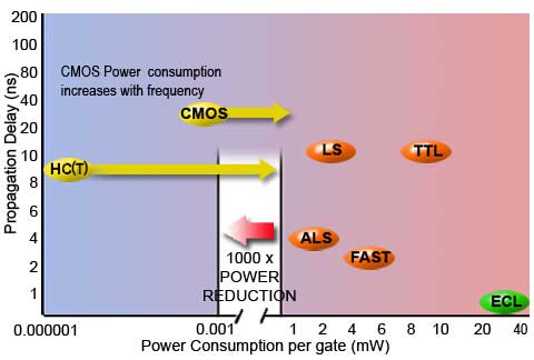
Fig 3.1.3 Logic Families Power vs Speed
As the overall performance of these families increased they also became more compatible. The increase in portable (battery powered) electronic devices along with the ability of chip manufacturers to make the component parts of ICs much smaller also meant that power could be reduced and speed increased.
Some of the main TTL and CMOS sub-families currently in use are compared in Fig. 3.1.3. Note how CMOS speed has been increased and power reduced with the introduction of the 74HC (High-speed CMOS) although (as the laws of physics demand), power consumption still increases, as the frequency at which they operate increases.
Because CMOS and TTL families can now operate at similar speeds and similar power consumption, the 74HCT (a CMOS sub-family compatible with TTL pinouts and voltage levels) now makes it possible to easily interface both families within in a single design, so enabling the use of the best features of each family.
74HC (and 74HCT for interfacing with the larger 74TTL families) are now recommended for most new designs.
The ECL Families
The ECL (Emitter Coupled Logic) families, originated in the late 1950s and remain the fastest chips available, but consume more power, and because they use a negative power supply (of −5.2V) have been difficult to interface with other families. This has changed with the introduction of PECL (Positive ECL) using a +5V supply, and LVPECL (Low Voltage Positive ECL) using a +3.3V supply. This now offers the opportunity of using mixed CMOS and TTL families at various power levels for logic operations and interfacing with ECL for high frequency digital communications.


