
Module 4.4
Depletion Mode MOSFETs.
- Section 4.4 The Depletion Mode MOSFET.
- • Depletion Mode MOSFET Operation.
- • MOSFE (IGFET) Circuit Symbols.
- • Applications of MOSFETS
- • High Power MOSFETS
IGFET).png)
Fig.4.4.1 Depletion Mode N Channel MOSFET
N Channel Depletion Mode MOSFET
The depletion mode MOSFET shown as a N channel device (P channel is also available) in Fig. 4.4.1 is more usually made as a discrete component, i.e. a single transistor rather than IC form. In this device a thin layer of N type silicon is deposited just below the gate-insulating layer, and forms a conducting channel between source and drain.
Therefore when the gate source voltage VGS is zero, current (in the form of free electrons) can flow between source and drain. Note that the gate is totally insulated from the channel by the layer of silicon dioxide. Now that a conducting channel is present the gate does not need to cover the full width between source and drain. Because the gate is totally insulated from the rest of the transistor this device, like other IGFETs, has a very high input resistance.
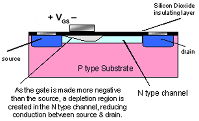
Fig.4.4.2 N channel depletion mode MOSFET operation
Depletion Mode Operation
In the N channel device, shown in Fig. 4.4.2 the gate is made negative with respect to the source, which has the effect of creating a depletion area, free from charge carriers, beneath the gate. This restricts the depth of the conducting channel, so increasing channel resistance and reducing current flow through the device.
Depletion mode MOSFETS are also available in which the gate extends the full width of the channel (from source to drain). In this case it is also possible to operate the transistor in enhancement mode. This is done by making the gate positive instead of negative. The positive voltage on the gate attracts more free electrons into the conducing channel, while at the same time repelling holes down into the P type substrate. The more positive the gate potential, the deeper, and lower resistance is the channel. Increasing positive bias therefore increases current flow. This useful depletion/enhancement version has the disadvantage that, as the gate area is increased, the gate capacitance is also larger than true depletion types. This can present difficulties at higher frequencies.
Depletion Mode MOSFET Circuit Symbols
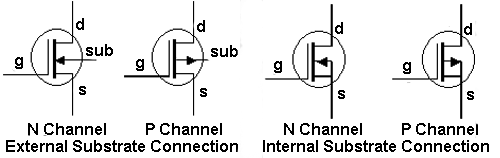
Fig.4.4.3 Circuit Symbols for Depletion Mode MOSFETs (IGFETs)
Notice the solid bar between source and drain, indicating the presence of a conducting channel.
Note: Making the gate more negative reduces conduction between source and drain In N channel devices, but increases conduction between source and drain In P channel devices.
Applications of FETs
Although FETs have a lower gain than bipolar transistors, their very high input impedance makes them suitable for applications where input signals may be severely reduced if applied to a bipolar transistor base that needs base current to operate. The planar technology used to make FETs is the same as that used to make integrated circuits, so most of the transistors found in I / Cs are of this type. A useful feature of FETs is that they tend to produce less background noise than Bipolar types and so are useful in the initial stages of systems such as amplifiers; radios etc. where signal levels are very small and could be swamped by excessive background noise.
High Power FETs
FETs used in high power output stages are often seen referred to as VMOS, DMOS or TMOS. These transistors are basically the same as other IGFETs but have specialised constructions that allow them to pass currents as large as 10A. They are also able to switch on and off very quickly (in nano seconds). This allows them to be used in such circuits as switch mode power supplies where very fast switching is essential.