
Module 4.5
Power MOSFETs
- After studying this section, you should be able to:
- Understand the operation of Power MOSFET switches.
- Recognise important characteristics of Power MOSFETS.
- Choose appropriate Power MOSFETs for switching DC current.
- Describe typical driver circuits for power MOSFETS in switching and controlling high current loads.
- Recognise typical safety measures to prevent damage due to over heating, over voltage or over current.
Fig. 4.5.1 Power MOSFETs
The Power MOSFET as a Switch
Both N and P channel Power MOSFETs (though mainly N channel) are widely used for switching DC loads of many types. They form the essential link between low power electronics and higher power 'real world' applications. Over recent years their use has grown enormously, replacing electro-mechanical relays to switch electrical loads in many applications. The load is switched on by applying a small voltage potential difference between the MOSFET Gate and Source, the actual value and polarity of this voltage depends on the MOSFET type chosen. When the MOSFET is used as a switch, it operates in 'saturation mode' and so conducts heavily when switched on. Because the current between Source and Drain (VDS) will be high, the resistance of the Drain to Source channel must be very low. Therefore if the power dissipated by the MOSFET, (and so its temperature) is to remain low, the resistance of the channel must typically be just a few milli-Ohms at a typical ambient temperature of 25°C. However this extremely low resistance will increase at higher temperatures.
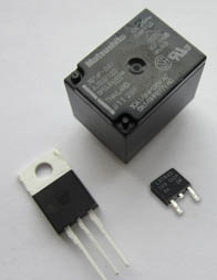
Fig. 4.5.2 Relay vs MOSFETs
The MOSFET vs a Relay
Unlike a mechanical relay or switch that has contacts either completely open or completely closed, a Power MOSFET provides an extremely high (but not infinite) resistance when in its 'off' mode, or an extremely low (but not zero) resistance (RDSon) when in its 'on' mode. The MOSFET is therefore basically a resistor whose value can be controlled by a small change in Gate/Source voltage (VGS). The actual value of the resistance between Drain and Source whilst the MOSFET is switched on is called RDSon. This is an important value because the Power MOSFET is designed to switch relatively large amounts of current and so whether it is 'on' or 'off' there will always be some resistance present, which will cause the MOSFET to dissipate some power as heat, and too much heat, (usually above 150 to 175°C) will be very likely to destroy the MOSFET.
Choosing a Power MOSFET
To ensure that this does not happen, having a clear understanding of the relationships beween Voltage, Current, Resistance and Power to enable selection of a suitable Power MOSFET for a particular application is important. There are hundreds of different types of Power MOSFETs produced by many manufacturers so selection can be difficult. Some power MOSFET designs are aimed at particular markets, for example high frequency switched mode power supplies need MOSFETs with a very high switching speed. Alternatively, computer driven control systems may require MOSFETs that have a lower than usual gate turn-on voltage to interface simply with 5V or 3.3V logic systems. Within each of these sub-groups there will be a choice of pin-out design. Surface mount types such as the D-PAK are often the most likely first choice but many types are still available in TO-220 packages as shown in Fig. 4.6.1. Making a reasoned choice for any application is a matter of studying a range of possible data sheets to identify suitable values for each of the following criteria.
Maximum Drain/Source Voltage (VDS)
This is normally one of the 'headline' criteria on many data sheets. Some high values for VDS are often claimed but it is important to remember that this figure is the absolute maximum voltage that the MOSFET can withstand between Drain and Source when in the 'off' condition. It is therefore generally considerably higher than the actual working voltage you would expect your chosen MOSFET to experience under normal working conditions, remember that with power switching applications there could always be the chance of unexpected voltage spikes etc. VDS should therefore be considered as a guide to long term reliability rather than a working voltage. As a rule of thumb the working voltage applied across Drain and Source should be no more than 80% of the maximum VDS.
Gate/Source Voltage (VGS)
The voltage applied between Gate and Source of a Power MOSFET to cause conduction between Source and Drain has two relevant values, firstly VGS(th) also called the Gate threshold voltage. This is a voltage applied to the Gate that will cause a current of 250µA to flow between Drain and Source. This is not intended to indicate a minimum turn on voltage, but is the voltage level the the Gate should be kept below while the MOSFET is held in its 'off' state. This minimises any leakage current between Source and Drain. To turn the MOSFET on the Gate/Source voltage should be considerably higher than VGS(th) but lower than the maximum allowed value for VGS. This maximum value may be a range of several volts, e.g. ±20V and is normally quoted in the data sheet for any particular MOSFET. In MOSFETs classed as 'Logic Level' the Gate/Source voltage will be +5V or less but in MOSFETs without this designation VGS will be higher. The ideal value chosen for a particular MOSFET will cause the Drain/Source Resistance (RDSon) to drop to a value that generates the minimum amount of wasted heat in the MOSFET whilst it is conducting.
Drain/Source Resistance (RDSon)
RDSon is one of the headline characteristics of MOSFETs and is crucial in designing switching circuits using Power MOSFETs. The greater the value of RDSon the more heat will be generated for a given value of Drain/Source current, therefore the lower the value of RDSon, the better. The value of RDSon also depends to some degree on Gate/Source voltage (VGS) and so manufactures will often quote several RDSon values for different operating conditions. Selecting the appropriate value of RDSon is the starting point in calculating the safe operating conditions in the design of a Power MOSFET switch circuit. Its value is greatly influenced by the Gate-Source Voltage (VGS), to much lesser extent by the Drain Current, but is closely linked to the temperature generated in the MOSFET.
Maximum Drain Current (ID)
Manufacturers usually quote the maximum drain current as one of their headline characteristics but it is important to remember that the headline maximum value is not normally a practical value but the maximum current under ideal cooling solutions with perfect thermal properties and the MOSFET on the verge of thermal breakdown. A more practical value for ID would be one related to calculated operating conditions that will keep the temperature of the MOSFET, (with or without a heat sink), below the maximum operating temperature, which is usually between 150°C and 175°C. Examples of typical calculations are given below.
Thermal Resistance (RthJC)
This characteristic describes the thermal resistance in degrees Celsius(°C) or degrees Kelvin(°K) per Watt of power dissipated between the transistor junction and the transistor case; for example 1.6 °K/W describes by how much the junction temperature of the MOSFET (in degrees Kelvin) will rise for every Watt of power dissipated. Various measures of Thermal Resistance can be used, depending on the type of device (transistor, MOSFET, IC etc.) to describe how efficiently the heat generated at a PN junction is transferred between the junction and the case, (subscript JC), between the junction and the air surrounding the Device (subscript JA) or, if a heat sink is used the different °K/W figures for each section of pathway across which heat is dissipated can be added to achieve a measure of the cooling efficiency; see more on heat sinks here. In many modern circuits where surface mount MOSFETS may be used different figures for RthJC may be used depending on the way the MOSFET is mounted, for example on a an area of copper print on the PCB or on a standard size of specifically designed PCB (e.g. a single layer 40mm square of flame retardant (FR-4) PCB mounted vertically in still air).
Typical Calculations for Using a MOSFET
When considering using a MOSFET as a switch, the amount of heat generated at its PN junctions is an important factor affecting the operation of the circuit and whether excessive temperature may affect its reliability. An example of how such calculations may inform the design of a circuit is given below, where a IRFZ44N MOSFET from International Rectifier (now Infineon) is used as a switch, to drive a 12V 36W automotive headlamp bulb from 5Vpp logic PWM signal. Although the MOSFET in this example is not suitable to be driven directly from a logic level input, the 12V 3A ouput circuit is totally isolated from the logic input via a 4N25 Opto Isolator which not only protects the input circuit, but also provides a 9Vpp square wave sufficient to drive the MOSFET gate.
The circuit providing a logic level output to drive the 4N25 in this case could be an Arduino running a simple pulse width modulation program that continually alters the brightness of the lamp, or a Pulse Width Modulator circuit based on discrete components including a 555 timer. The circuit, shown in Fig. 4.6.2 easily drives the 3A resistive load without any excessive heating.
The circuit could possibly drive higher current loads with or without adding a heat sink but since 12V at 3A is also the limit of my bench power supply, further investigation was not possible.
The Power MOSFET Drive circuit requires a series of choices and calculations. The MOSFET chosen to control the brightness of a 12V DC incandescent lamp is based on the following criteria:
1. The Maximum VDS voltage of the MOSFET must be greater than 12V by a margin to allow for any supply voltage variations, so a MOSFET with a maximum DC voltage of 55V seems reasonable.
2. A low RDSon value is important to prevent excessive heating of the MOSFET.
3. As the MOSFET is to be driven from a logic circuit via 4N25 opto-isolator, logic compatibility is not needed. However if isolation is not a priority, a similarly specified MOSFET can be used, but it must be compatible with a logic level drive.
4. The package type should be available as a through hole mounting TO-220 as the prototype is to be built on strip-board.
Starting with these basic criteria in mind, the IRFZ44N was chosen. The next task is to check that the chosen MOSFET is up to the job. This requires some calculations based on information gathered from the manufacturer's data sheet.
From the IRFZ44N data sheet:
RDSon (for VGS = 10V) = 17.5mΩ
De-rated by adding 20% = 21mΩ
Power Dissipated = I2R
Lamp Current (on) = 3A (Supply Voltage = 12V, Lamp Rated Power = 36W)
Power Dissipated in the MOSFET = I2 x RDSon = 32 x 21mΩ = 189mW
Thermal Resistance (junction to case) of the MOSFET with no heat sink (RTHJC) =1.5°C per Watt
Therefore estimated junction temperature with Ambient Temperature (TA) =25° = (1.5 x RTHJC) + TA
= (1.5 x 189 E-3) +25 = 25.28°C
Therefore as maximum safe operating temperature for the IRFZ44N is 175°C (or °K) and the forecast rise in Junction Temperature is only 0.28°C (25°C to 25.28°C) the MOSFET can be safely operated without a heat sink. However these calculations are based on the MOSFET alone and do not wholly take into consideration the effect of the external components and how they interface with the MOSFET. Working examples of this design process and how it can be applied to practical switching circuits are described in Module 4.6 MOSFET Switches.