
Module 7.3
Testing Transistors.
- Section 7.3 Testing Transistors
- •The Two Diode Model for BJTs .
- •Identifying Transistor Connections.
- • Testing BJTs.
- • Testing JFETs.
- • Testing MOSFETs
The Two Diode Transistor Model
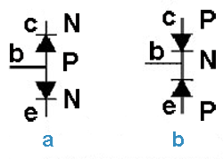
Fig.7.3.1 The Two Diode Transistor Model.
As shown in Fig.7.3.1 whether a transistor is (a) an NPN type or (b) a PNP type bipolar transistor, it consists of two diode junctions, the base-emitter junction and the base-collector junction. For the purposes of testing, these can be thought of as simply as two diodes with one common connection i.e. the base. So to test a transistor you just need to check the forward and reverse resistance of each of these junctions. However to do this it is first necessary to find out which pin is which.
Plan A - Use The Manufacturer's Data Sheet
The best way to check the functions of the pins is to use the manufacturer's datasheet, just about every transistor ever made has its own datasheet on the Internet. Just type the transistor number in internet search bar and you should find a selection of sites publishing the data you need. You also should find a diagram in the datasheet showing the transistor pin connections (pinouts) where the collector, base and emitter pins and any variants are shown. In the off chance that you can't find the right information it will be necessary to resort to Plan B.
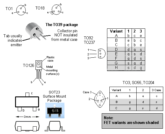
Fig.7.3.2 Common Transistor Packages.
Plan B - Finding The Pin Functions by looking at the transistor package information.
What if you can't find the vital transistor identity number on the transistor itself? All is not lost; you can still find the pin functions by a little detective work. If the transistor you are testing has a metal case, such as in the layout plans for the common encapsulations TO18, TO3, TO126, TO202 TO72 etc., that's helpful. A metal case or heat sink area is almost always connected to the collector so that the heat is dissipated easier. This means that if you measure the resistance from the case or the metal mounting area to each pin in turn, the one pin that measures zero ohms is the collector. What we really need to find however is the base. In transistor packages such as the TO39 that's easy; the emitter is nearly always next to the metal tab and the collector is connected to the can.
Notice that often this makes the base the centre of the three connections - but this is not always the case; don't rely on the base being at the centre. Study the common package types illustrated in Fig.7.3.2. There are variations even within the same type of package. So if Plan B has not solved the puzzle, no worries, there is always Plan C.
Plan C - Testing Transistors With Unknown Pinouts.
Another useful way to find the base however is to measure the resistance between the various pins. Imagine to begin with that we suspect an unknown transistor may be a NPN type (these are far more common than PNP in modern circuits), and it may be faulty
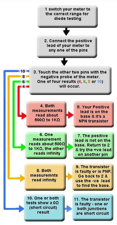
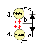
Fig.7.3.3 Identify Transistor Pinouts and Find
Faulty Transistors.
Using the Fault Finding Chart
Follow the instructions in boxes 1, 2 and 3
If you are guided to go to box 4, and both tests give a reading of between 500Ω and 1KΩ well done! You have found the base pin at first attempt, and box 5 tells you that you are testing a NPN transistor.
Alternatively, if both measurements indicate infinity you are guided to box 6 as your positive lead was not on the base. So go back to test 2 and try again with your positive lead on another pin. Repeat this test until you have found the base pin.
Or, if both measurements in step 4 read infinity, either the transistor is faulty (one or both junctions are open circuit) or the transistor is a PNP type. Therefore you need to start again, but this time using the negative meter lead to find the base pin.
If, in test 3 one or both test indicate 0Ω (short circuit) and you haven't accidentally touched the positive and negative leads together during you tests, the transistor is fault with one or both junctions short circuit.
The fault finding chart will test a bipolar transistor whether you know which pins are which or not, but-
If You Already Know The Pinouts
Here is a short-cut version for confirming if a known transistor is faulty or not. If all of the tests pass as correct, the transistor is OK. If any tests fail, the transistor is for the rubbish bin.
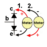
1. Test the resistance between collector and emitter.
2. Then reverse the positive and negative meter connections. If the transistor is good there should be an infinity reading both ways.
Now connect the positive meter lead to the base and test the resistance of both junctions by connecting the negative meter probe (3) to the collector, and then (4) the emitter. You should get a typical forward resistance reading of between 500Ω and 1KΩ in both cases.
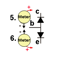
Finally reverse the meter connections so that the negative lead is connected to the base. Connect the positive probe (5) to the collector, then (6) to the emitter. Both junctions should now read infinity.
Testing JFETs
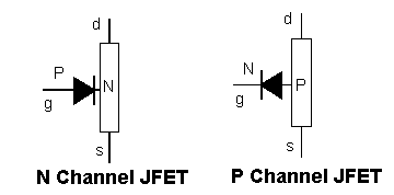
Fig.7.3.4 The JFET Diode Model
JFETs are constructed differently to Bipolar Transistors and so require a different testing techniques. First consider the JFET diagrams in Fig 7.3.4 which show the drain/source path as a single block of either N type or P type silicon and the Gate as a simple diode which has either it's anode (in P Channel JFETs) or cathode (in N Channel JFETs) connected directly drain/source path. Therefore instead of having to test two PN junctions as in BJTs, in JFETs we only need to test one junction.
The first thing to know before testing a suspect JFET is the pinout, like any other transistor this can be obtained by downloading the data sheet for the particular JFET of interest.
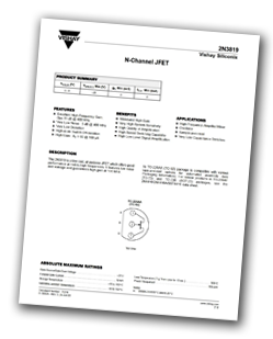
Fig.7.3.5 2N3819 Datasheet.
Once the Source, Drain and Gate pins are identified, the following digital meter tests should reveal the state of the JFET:
- 1. Switch the meter to diode testing mode.
- 2. Measure the resistance between Source and Drain with the positive meter lead on the Drain pin.
- 3. Reverse the meter leads (positive to Source) and read the resistance again.
The results of tests 1. and 2. should typically be around 130Ω to 180Ω but this can vary in different JFETS. If the resistance seems suspiciously low, it could mean that there is a remnant of voltage on the very high impedance Gate due to the gate junction capacitance. To remove this possibility short circuit the Gate and Source by momentarily touching both pins together then repeat tests 1. and 2. A reading of 0Ω or infinity means the JFET is faulty.
- 4. Assuming steps 2 and 3 are OK, check the resistance between Gate and Source with the positive meter probe on the Gate pin. Expect a resistance of around 700Ω to 1KΩ. This is the forward resistance of the Gate diode.
- 5. Keeping the positive meter probe on the Gate, move the negative probe to the Drain and check the resistance between Gate and Drain. Expect similar results to test 4.
- 6. Now reverse the meter connections and test the reverse resistance of the Gate diode by placing the negative probe on the Gate pin and the positive probe on the Source pin. The resistance now should be infinity.
- 7. Finally check the Gate to Drain resistance by leaving the negative probe on the Gate and moving the positive probe to the Drain pin. Again the reading should be infinity.
Fig.7.3.6 JFET in
Anti-Static Foam.
With all of these tests you should refrain from handling the JFET as much as is possible. Ideally, when working with any type of field effect transistors you should be working at an ESD (Anti Static Discharge) workstation or be wearing an antistatic wrist strap. Alternatively you could at least stick the pins (assuming they are long enough) in a piece of anti static foam such as FETs are normally stored in. The resistance between the pins will then avoid the build up of static voltages, but will be high enough not to greatly affect the resistance readings you take during these tests.
Testing MOSFETS
The first thing to realise about MOSFETs is that they are much more sensitive to damage by static discharge than any other types of transistor, even JFETs. This is due to the fact that MOSFETs are insulated gate transistors, so the gate is totally isolated from the Drain/Source pathway. This means that some considerable capacitance exists between the gate and the other terminals. This capacitance can easily be charged up to any voltage including extremely high voltages that can be present on the human (your) body by simply walking across a carpeted room for example. Such static voltages can easily destroy a MOSFET. Therefore care must be taken at the outset to avoid touching any of the MOSFET terminals when the MOSFET is not in its anti static packaging or connected into a circuit. For the purposes of these tests therefore, we will assume that the tester (you) will be using anti static techniques as outlined in the section on JFET testing. However one precaution we cannot use is to insert the MOSFET into anti static foam; as this will prevent our tests from working. Therefore to carry out the tests we will avoid touching the MOSFET pins as much as possible and insert the pins into a breadboard.
The MOSFET Test Sequence
Fig.7.3.7 MOSFET-on-Breadboard.
- 1. Set the digital multi-meter to the diode test position.
- 2. Momentarily short the Gate and Drain terminals together with one of your meter probes to discharge any gate capacitance.
- 3. Connect the positive meter probe to the Drain terminal and the negative probe to the Source terminal. The meter should read infinity.
- (If the meter reads 0Ω try shorting Gate and Drain again with the negative meter lead to ensure any gate charge is removed).
- Connect the positive meter lead to the Source and the Negative probe to the Drain terminal. The meter should now read about 500Ω
- What you have now tested is the reverse and forward resistance of the MOSFET's internal protection diode.
- 4. Now connect the negative meter probe to the Source terminal and momentarily touch the gate terminal with the meter positive probe. This will momentarily charge the base capacitance sufficiently to switch the MOSFET on.
- 5. Connect the positive probe to the drain and the negative probe to the source (Repeating test 3). This time the meter should read 0Ω because the MOSFET is now switched on by the voltage you applied to the gate.
- 6. Reverse the meter leads (positive to Source and negative to Drain) Again the Drain/Source resistance should be 0Ω confirming that the MOSFET is switched on.
- 7. To switch the MOSFET off, use either probe to momentarily short Gate to Drain.
- 8. Check that the MOSFET is now 'off' placing the positive probe on the Drain terminal and the negative probe on the Source to check that the resistance between Drain and Source is infinity once more showing that with zero volts on the Gate, the MOSFET is now switched off and the MOSFET is working correctly.
Conclusion.
Carrying out the tests of JFETs or MOSFETs will help you identify faulty FETs and better understand Field Effect Transistors, but are also meant to compliment your studies of these components. For more detailed information look at Semiconductors Module 4 (Field Effect Transistors) to complete your studies of these important components.
Warning: You should never work on "live" circuits unless you know AND USE safe working practices. Many circuits that derive power from the mains (line) supply (and some that don´t) contain LETHAL voltages as well as other hazards. Live circuits must only be worked on by fully trained personnel. Before attempting any work on live circuits using any information provided on this web site, please read the important DISCLAIMER.