
Module 2.1
Digital Logic
- After studying this section, you should be able to:
- Describe the action of logic gates.
- • AND, OR, NAND, NOR, NOT, XOR and XNOR.
- • Using Boolean expressions.
- • Using truth tables.
- Understand the use of universal gates.
- • NAND.
- • NOR.
- Recognise common 74 series ICs containing standard logic gates.

Logic Gates
Seven Basic Logic Gates

Fig. 2.1.1 ANSI & IEC Gate Symbols
Digital electronics relies on the actions of just seven types of logic gates, called AND, OR, NAND (Not AND), NOR (Not OR), XOR (Exclusive OR) XNOR (Exclusive NOR) and NOT.
Fig. 2.1.1 illustrates a selection of the basic logic gates that are available from a number of manufacturers in standard families of integrated circuits. Each logic family is designed so that gates and other logic ICs within that family (and other related families) can be easily combined, and built into larger logic circuits to carry out complex functions with the minimum of additional components.
In binary logic there are only two states allowed, 1 and 0 or ‘on and off’. the word NOT in the world of binary logic therefore means ‘the opposite of’. If something is not 1 it must be 0, if it is not on, it must be off. So NAND (not AND) simply means that a NAND gate performs the opposite function to an AND gate.
A logic gate is a small transistor circuit, basically a type of amplifier, which is implemented in different forms within an integrated circuit. Each type of gate has one or more (most often two) inputs and one output.
The principle of operation is that the circuit operates on just two voltage levels, called logic 0 and logic 1. These values are represented by two different voltage levels. In 5 volt logic, 1 is ideally represented by 5V and 0 by 0V, and in 3.3V logic 1 is ideally represented by 3.3V and logic 0 by 0V. When either of these voltage levels is applied to the inputs, the output of the gate responds by assuming a 1 or a 0 level, depending on the particular logic of the gate. The logic rules for each type of gate can be described in different ways; by a written description of the action, by a truth table, or by a Boolean algebra statement.
Boolean Statements

Fig. 2.1.2 Boolean Symbols for Gates
The actions of any of these gates can also be described using Boolean statements. These use letters from the beginning of the alphabet, such as A, B, C etc. to indicate inputs, and letters from the second half of the alphabet, very commonly X or Y (and sometimes Q or P) to label an output. The letters have no meaning in themselves, other than just to label the various points in the circuit. The letters are then linked by a Boolean symbol indicating the logical action of the gate.
The • symbol indicates AND although in many cases the • may be omitted. (A•B may also be written as AB or A.B)
+ indicates OR
⊕ indicates XOR (Exclusive OR)
Although the symbols • and + are the same as those used in normal algebra to indicate product (multiplication) and sum (addition) respectively, in binary logic the + symbol does not exactly correspond to sum. In digital logic 1 + (OR) 1 = 1, but the binary sum of 1 + 1 = 102, therefore in digital logic + must always be considered as OR.
Three further types of logic gate give an output that is an inverted version of the three basic gate functions listed above, and these are indicated by a bar drawn above a statement using the AND, OR, or XOR symbols to indicate NAND, NOR and XNOR.
A•B means A AND B but A•B means A NAND B
The action of any of the gates can therefor be described by using its Boolean equation.
For example, an AND gate gives an output of logic 1 when input A AND input B are at logic 1, but a NAND gate would give a logic 0 output for the same input conditions. Also where the AND gate gives a logic zero for a particular input combination, the NAND gate would give a logic 1. The ‘N’ in the gate’s name, or the bar above the Boolean expression therefore indicates that the output logic is ‘inverted’. In digital logic NAND is ‘NOT’ AND, or the opposite of AND. Similarly NOR is ‘NOT’ OR, and XNOR is ‘NOT’ XOR.
Describing the Action of Logic Gates
Alternatively the action of any of the 7 types of logic gate can be described using a written description of its logic function.
- The AND gate output is at logic 1 when, & only when all its inputs are at logic 1, otherwise the output is at logic 0.
- The OR gate output is ate logic 1 when one or more of its inputs are at logic 1. If all its inputs are at logic 1 , the output is at logic 0.
- The NAND gate output is at logic 0 when & only when all its inputs are at logic 1. Otherwise the output is at logic 0.
- The NOR gate output is at logic 0 when one or more of its inputs are at logic 1. If all of its inputs are at logic 0, the output is at logic 1.
- The XOR gate output is at logic 1 when and only one of its inputs is at logic 1. Otherwise the output is at logic 0.
- The XNOR gate output is at logic 0 when one and only one of its inputs is at logic 1 Otherwise the output is at logic 1. (It is therefore similar to the XOR gate, but its output is inverted).
- The NOT gate output is at logic 0 when its only input is at logic 1, and at logic 1 when its only input is at logic 0. For this reason it is often called an INVERTER.

Fig. 2.1.3 Truth Tables
Truth Tables
Another useful way to describe the action of a digital gate (or a whole digital cicuit ) is to use a truth table. Each table consists of two or more columns, one column for each input or output; the number of lines in the column will be enough to record all possible logic states for that input or output. Fig.2.1.3 illustrates two typical truth tables for ciruits of different levels of complexity.
The top table is for a simple two input and gate. This has two inputs labelled A and B and one column (X) for the output. Comparing the truth table with the written description in "Describing the Action of Logic Gates" (above) it can be seen that the truth table follows the written description by showing that output X is at logic 1 only when inputs A and B are at logic 1, otherwise (where the three upper lines are 00, 01 and 10) the output is logic 0.
The second table in Fig.2.1.3 describes a more complex circuit (of five NAND gates mimicing a XOR gate). Notice that now the truth table is expanded to illustrate the logic levels at four further inputs or outputs in addition to inputs A and B before the final output X is illustrated in the right hand column. Such complex tables can be of great value in both digital circuit design or fault finding.
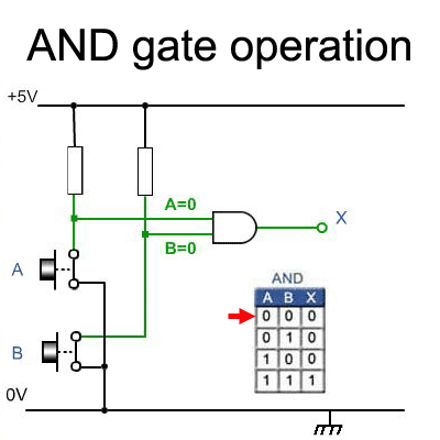
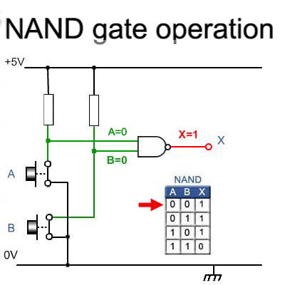
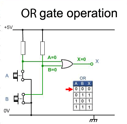
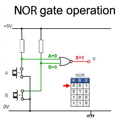
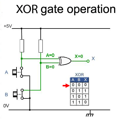
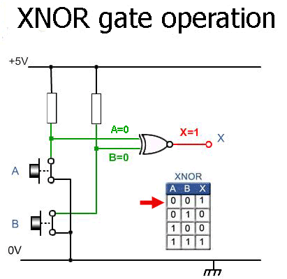
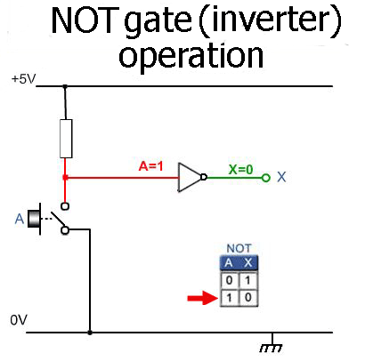
Fig.2.1.4 Logic Gate Animations (Click any gate)
Logic Gate Animations
In Fig 2.1.4 you can check out the operation of the basic logic gates for yourself. The gate animations allow you to choose any one of the 7 basic gates and see a new page with an animated image of the gate in operation. Use the animation to become familiar with the operation of each of the gates. To return to this page, just close the page showing the animation.
To easily understand more complex digital circuits it is important to develop a good mental picture of the expected output from each gate for any possible input.
The animations available in Fig.2.1.4 also show how the seven basic logic functions can be described using a ‘truth table’ to show the relationship between the output (X) and all possible input combinations for inputs A and B, shown as a four value binary count from 00 to 11. Each animated diagram shows the input and output conditions for one of the seven logic functions in its two input form. Some types of gate however, are also available with more (e.g. 3 to 13) inputs. For these gates the truth tables would need to be extended to include all possible input conditions.
Universal Gates
Because gates are manufactured in IC form, typically containing two to six gates of the same type, it is often uneconomical to use a complete IC of six gates to perform a particular logic function. A better solution may be to use just a single type of gate to perform any of the logic operations required. Two types of gate, NAND and NOR are often used to perform the functions of any of the other standard gates, by connecting a number of either of these ‘universal’ gates in a combinational circuit. Although it may not seem efficient to use several universal gates to perform the function of a single gate, if there are a number of unused gates in one or more NAND and NOR ICs, these can be used to perform other functions such as AND or OR rather than using extra ICs to perform that function. This technique is especially useful in the design of complex ICs where whole circuits within the IC can be fabricated using a single type of gate.
Fig. 2.1.5 a to g shows how NAND gates can be used to obtain any of the standard functions, using only this single gate type.
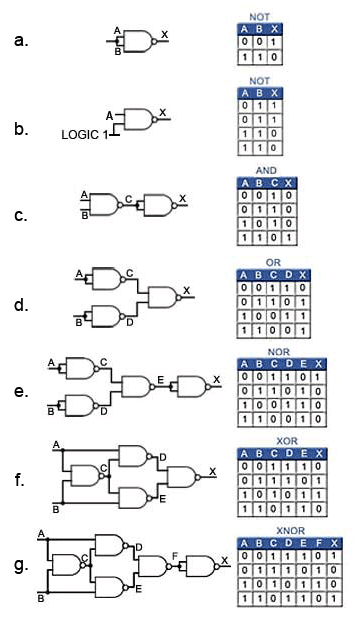
Fig 2.1.5 Creating any Logic Function Using NAND Gates
NOT Function
a. Connecting the inputs of the NAND gate together creates a NOT function.
b. Alternatively the NOT function can be achieved by using only 1 input and connecting the other input permanently to logic 1.
AND Function
c. Adding the NOT function (an inverter) to the output of a NAND gate creates an AND function.
OR Function
d. Inverting the inputs to a NAND gate creates an OR function.
NOR Function
e. Using a NOT function to invert the output of an OR function creates a NOR function.
XOR function
f. Four NAND gates (a single IC) connected as shown creates an XOR function (and a Quad NAND IC is about 15% cheaper than a Quad XOR IC).
XNOR Function
g. Inverting the output of the XOR function creates an XNOR function.
Similar conversions can be achieved using NOR gates, but as NAND gates are generally the least expensive ICs, the conversions shown in Fig. 2.1.5 are more frequently used. The reason for such conversions is usually cost. This may not seem very useful since none of the basic 74 series ICs are expensive, but when several thousand units of a particular circuit are to be manufactured, the small savings in cost and space on printed circuit boards by maximising the use of otherwise unused gates in multi gate ICs can become very important.
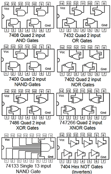
Fig. 2.1.6 Logic Gates From the 74 series TTL IC Family
Logic ICs
Typically, standard logic gates are available in 14 pin or 16 pin DIL (dual in line) chips. The number of gates per IC varies depending on the number of inputs per gate. Two−input gates are common, but if only a single input is required, such as in the 7404 NOT(or inverter) gates, a 14 pin IC can accommodate 6 (or Hex) gates. The greatest number of inputs on a single gate is on the 74133 13 input NAND gate, which is accommodated in a 16 pin package.
Data Sheets
7404 Hex NOT gates (Inverters)