Module 2.3
Boolean Algebra
- After studying this section, you should be able to:
- Describe logic circuits using Boolean equations.
- • Create Boolean expressions for intermediate gate outputs.
- • Use complex Boolean equations to describe complete logic circuits.
- Simplify Boolean equations using Boolean laws.
- • Commutative.
- • Associative.
- • Distributive.
- • Identity.
- • Complement.
- • Duality.
- • De Morgan‘s Theorem.
- Use De Morgan‘s theorem to convert multiple gate circuits to universal gates.
Boolean Algebra
Digital Electronics Module 2.1 showed that the operation of a single gate could be described by using a Boolean expression. For example the operation of a single AND gate with inputs A and B and an output X can be expressed as:
X = A•B
Note:
The symbol • represents a logical AND, but because the use of special symbols can be inconvenient in printed material, the AND symbol is often omitted, as in AB or separated by a full stop as in A.B as used to indicate multiplication in standard algebra. The multiplication symbols x and * can also be seen in some texts, because the logical AND is similar to binary multiplication, (but not the same when numbers having more than one-bit are used). Module 2.2 showed the relationship between a truth table that describes the operation of a circuit, and a Boolean equation that describes the logic of the circuit.
A combinational logic circuit such as that shown in Fig 2.3.1 (a repeat of Fig 2.2.2) is described by a Boolean equation as:
X = (A•B) + (A•C) + (A•B•C)
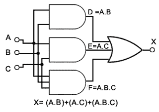
Fig. 2.3.1 Three Input Circuit with Redundant Gates
This could also be written (less clearly) as "The output X will be 1 when A and B or A and C or A and B and C are 1, otherwise X will be 0".
However Module 2.2 also showed that although a Boolean equation may give an accurate description of a logic process described by a truth table, it might require simplification before being interpreted as an actual circuit. The circuit shown in Fig 2.3.1 was simplified in Module 2.2 by closely examining a truth table to find redundant gates. However, with anything but the simplest circuits this can be tedious and it is easy to make mistakes.
This module therefore describes methods for simplifying Boolean equations directly, using Boolean algebra, rather than by the use of truth tables.
Circuit Simplification Using Boolean Algebra
The algebraic method used to simplify digital circuits applies a number of Boolean laws to successively simplify complex equations. Selected laws and rules are applied, step by step, to the original equation, so as to eventually arrive at a simplified version that can be implemented with a smaller number of gates and therefore lead to a simpler circuit.
Boolean Laws
The laws of Boolean algebra are similar in some ways to those of standard algebra, but in some cases Boolean laws are unique. This is because when logic is applied to digital circuits, any variable such as A can only have two values 1 or 0, whereas in standard algebra A can have many values.
Commutative Laws
In a group of variables connected by operators AND or OR, the order of the variables does not matter.
1a. Boolean addition (OR): A+B = B+A
1b. Boolean multiplication (AND): A•B = B•A
Associative Laws
The order of calculation can be changed without affecting the result (Change which terms are in brackets, or remove brackets). Note: This is only OK so long as all signs (+ or •) are the same.
2a. Boolean addition (OR): (A+B)+C = A+(B+C) = A+B+C
2b. Boolean Multiplication (AND): (A•B)•C = A•(B•C) = A•B•C = ABC
Distributive Laws
The same answer is arrived at when multiplying (ANDing) a variable by a group of bracketed variables added (ORed) together, as when each multiplication (AND) is performed separately.
Law 3a is similar to factoring in normal algebra, but law 3b is unique to Boolean algebra because unlike normal algebra, where A x A=A2, in Boolean algebra A•A = A
3a. A•(B+C) = A•B+A•C
3b. A+(B•C) = (A+B) • (A+C)
Identity Elements
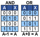
In rule 4a, when the variable A is ANDed with logic 1 (called the Identity Element for the AND operator). The variable ANDed with 1 retains its identity.
Rule 4b, shows that the Identity Element for the OR operator is 0, and any variable (e.g. A) ORed with 0 it retains its identity.
4a. A•1 = A
4b. A+0 = A
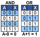
5a and 5b show how by ‘forcing the Identity Element’, (in B column of the truth tables) to the opposite states to those used in 4a and 4b, produces an output that is the same as the Identity Element.
5a. A•0 = 0
5b. A+1 = 1
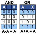
6a and 6b show that ANDing or ORing two identical variables, produces an output equal to a single variable, showing that one of the variables is redundant, a useful rule when simplifying Boolean equations.
6a. A•A = A
6b. A+A = A
Complement Law
7a. A + A = 1 Any variable ORed with its inverse is 1
7b. A • A = 0 Any variable ANDed with its inverse is 0

Reduction
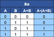
8a. When a single variable (A) is ANDed with itself OR a second variable (A+B), the result is equal to the single variable.
8a A•(A+B) = A
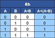
8b. When a single variable (A) is ORed with itself AND a second variable (A•B), the result is equal to the single variable.
8b A+(A•B) = A
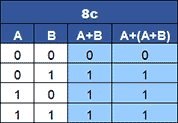
8c. When a single variable (A) is ORed with itself OR a second variable (A+B), the single variable disappears.
8c A+(A+B) = (A+B)
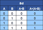
8d. When a single variable (A) is ANDed with itself AND a second variable (A•B), the single variable disappears.
8d A•(A•B) = (A•B)
Duality Rules
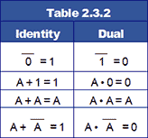
It is possible to derive additional identities by obtaining the Dual of an identity. This involves changing the AND operators to OR and the OR operators to AND. Additionally any 0s are changed to 1s and 1s to 0s as shown in Table 2.3.2.
The duality rule can be used to change a logic expression containing both AND and OR elements to its equivalent dual expression.
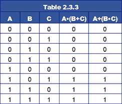
Table 2.3.3 shows that A•(B+C) is the same as A+(B•C).
Simplifying Boolean Equations
Minimising complex Boolean expressions to their simplest form using Boolean laws and rules is a matter of choosing the most appropriate law or rule to reduce the expression step by step. If the resulting minimisation is correct, the minimised equation and the original equation should give identical output columns when truth tables for the original and minimised circuits are compared.
These Boolean algebraic methods would normally be used on logic circuits with just a few gates and only two or three inputs, as this method of simplification becomes more difficult and cumbersome to use when more gates or inputs are involved.
Which laws are applied to change an equation, and in what order is a matter of practice and intuition. This method involves looking at the original complex equation and selecting a law that will simplify a particular part, so obtaining a simpler equation, and then choosing another law that will simplify the equation further, and so on until the equation can no longer be made simpler.
There is no simple algorithm to specify the order of steps to be taken and several routes may be taken to reach the goal of a simplified and ideally minimised circuit.
Whether the result is also the minimum possible circuit can only be judged by looking for any possible further reduction using the Boolean laws.
In practice, small circuits with just two or three inputs can very often be simplified just by looking at the truth table and picking out any redundant logic combinations, as shown in Table 2.2.2 in Module 2.2 (Combinational Logic), but Boolean simplification is useful for more complex circuits.
Boolean Simplification Examples
Example 1
Suppose the cash room at a store has access restricted to certain employees, each of whom has a key, which produces a logic 1 at particular inputs to an unlocking circuit.
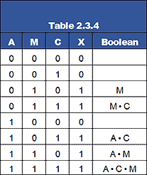
Only the store manager (M) can enter alone. The assistant manager (A) and the cashier (C) also have access, but only when accompanied by each other, or by the store manager. Design a combinational logic circuit that will allow access by producing a logic 1 when the above conditions are met.
Truth table
The conditions requiring a logic 1 output can be arranged as a truth table (Table 2.3.4) and Boolean expressions can be derived from the truth table for each input combination that produces a logic 1 output.
The five Boolean expressions can be separated by OR operators to form a complete Boolean equation.
X = M + M•C + A•C + A•M + A•C•M
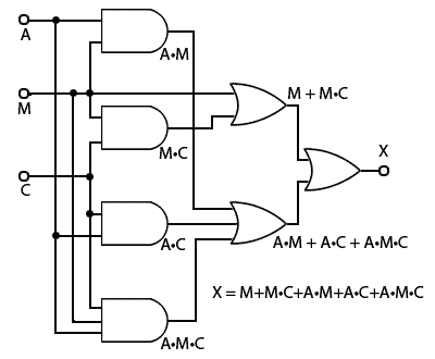
Fig. 2.3.2 Cash Room Access Circuit
This suggests a circuit like that shown in Fig. 2.3.2, which would require four I.Cs:
1x 74HCT08 2 input AND (containing 4 gates).
1x 74HCT10 3 input AND (containing 3 gates).
1x 74HCT32 2 input OR (containing 4 gates).
1x 74HCT4075 3 input OR (containing 3 gates).
However, by choosing appropriate laws and rules from those listed above, the circuit can be considerably simplified.
Starting with the equation derived from Table 2.3.4:
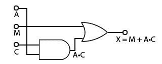
Fig. 2.3.3 Simplified Cash Room Access Circuit
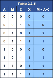
X = M + M•C + A•C + A•M + A•C•M
Since M + M•C = M (Reduction rule 8b)
X = M + A•C + A•M + A•C•M
And as M + A•C + A•M = M + A•M + A•C (Commutative Law 1a)
X = M + A•M + A•C + A•C•M
And as M + A•M = M (Reduction rule 8b)
X = M + A•C + A•C•M
And as M + A•C + A•C•M = M + A•C•M + A•C (Commutative Law 1a)
X = M + A•C•M + A•C
And as M + A•C•M = M (Reduction rule 8b)
X = M + A•C
No further reduction possible.
The simplified circuit is shown in Fig 2.3.3, which provides exactly the same function as Fig. 2.3.2. This can be confirmed by comparing the simplified equation X = M + A•C with the original column X in Table 2.3.5.
The simplified circuit in Fig 2.3.3 still requires two I.Cs, (AND and OR) and it now only uses one gate per chip. Unless the spare gates are to be used elsewhere in another part of the circuit, this is still wasteful.
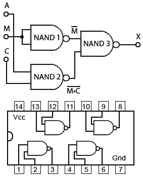
Fig. 2.3.4 NAND only Cash Room Access Circuit
A better option could be to replace the AND and OR functions with universal gates such as NOR or NAND. A ‘NAND only’ version of the simplified circuit is shown in Fig. 2.3.4. This version uses three gates instead of two, but all the gates are the same and can be accommodated within a single 7400 IC. The original circuit has therefore now been reduced from four ICs to one.
Operation
NAND 1 has both its inputs connected together, which converts it to an inverter or NOT gate and therefore produces Mat its output. NAND 2 works as an AND gate with its output inverted and so produces an output of A•C. The Boolean expression for the circuit using NAND gates now becomes:
X = M + A•C
This is because of the application of another very useful Boolean algebra law, De Morgan’s Theorem. Before looking at how the theorem works, note the difference in the use of the inversion bars in Boolean expressions. This is an important feature in the application of De Morgan’s Theorem:
A broken bar A•B indicates that the inputs (to an AND gate for example) are inverted, whilst an unbroken bar A•B indicates an inverted output.
De Morgan’s Theorem
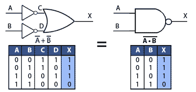
Fig. 2.3.5 De Morgan’s Law 1
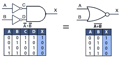
Fig. 2.3.6 De Morgan’s Law 2
Augustus De Morgan formulated an extension to George Boole’s Algebraic logic that has become very important in digital logic. Not only is it used in the simplification of Boolean expressions but can also be used to change the function of logic gates, so that NAND gates (or NOR gates) can carry out any of the other standard logic functions of gates. The theorem comprises two laws that describe how inverting the inputs to a gate, changes the gate’s function.
Law 1.
A + B = A • B Inverting the inputs to an OR gate changes its function to NAND.
Law 2.
A • B = A + B Inverting the inputs to an AND gate changes its function to NOR
Considering these two equalities the other way round, A + B = A • B De Morgan’s Theorem is often described as "Break the bar and change the sign." Meaning that by placing, or removing the bar above the AND or OR operator (• or +) the operator is inverted. Therefore the complement of the AND function is OR.
Applying De Morgan’s Theorem
These equalities, generally called De Morgan’s Laws 1 and 2 are illustrated in Fig. 2.3.5 and Fig. 2.3.6 as they apply to AND, NOR, NAND and OR gates. Note however, that when De Morgan’s theorem is applied to the XOR and XNOR gates there is no change in the gate’s function.
The usefulness of De Morgan’s theorem when applied to circuits can be seen by comparing Fig. 2.3.3 and Fig. 2.3.4 where it was instrumental in changing the functions of the AND and OR gates in Fig.2.3.3 to all NAND gates in Fig. 2.3.4, so the circuit can be made using one IC instead of two.
Inverting the Inputs
In Fig. 2.3.4 an additional gate NAND 1 appears in the circuit, and has its two inputs connected together to act as a NOT gate (check this by looking at the truth table for a NAND gate in Fig. 2.3.5), when both inputs are the same (row 1 and row 4) the output (X) is an inverted version of the inputs (A•B).
This additional gate in Fig. 2.3.4 provides M at the top input to NAND 3 instead of the M applied to the top input of the OR gate in Fig 2.3.3.
NAND 2 in Fig. 2.3.4 replaces the AND gate in Fig 2.3.3 so that the bottom input to NAND 3 is now A•C instead of A•C.
Therefore inputs to NAND 3 are now M and M•C. Therefore both inputs to NAND 3 have been inverted (without actually using any NOT gates) to make NAND 3 act, according to De Morgan’s theorem, as an OR function, so giving the correct output of X = M + A•C.
Summary
Boolean algebra gives a more compact way to describe a combinational logic circuit than truth tables alone. It can also be used for simplification of circuits, however this can also be cumbersome and error prone. When circuits with more than two or three inputs are involved a better method of circuit reduction that works well with circuits having up to four or six inputs is the Karnaugh Map.


