
Module 2.2
Combinational Logic & Truth Tables
- After studying this section, you should be able to:
- Describe complex logic functions.
- • Using truth tables.
- • Using Boolean expressions.
- Understand the relationship between truth tables and logic circuits.
- • Analyse simple digital circuits using truth tables.
- • Formulate Boolean equations from truth tables.
- • Use truth tables to simplify logic circuits.
Combinational logic
Combining a number of basic logic gates in a larger circuit to produce more complex logical operations is called combinational logic. Using such circuits, logical operations can be performed on any number of inputs whose logic state is either 1 or 0 and this technique is the basis of all digital electronics.
Combinational logic circuits can vary in complexity from simple combinations of two or three standard gates, to circuits containing hundreds of thousands, or even millions of gates. It is this ability to combine just a few simple gate circuits, which can be manufactured to microscopic dimensions, but in almost limitless combinations that makes digital electronics so powerful.
To understand the operation of a combinational logic circuit, and what logic state should be present at any particular point in the circuit, it is necessary to accurately analyse the operation of the circuit. For this purpose, several methods can be used, depending on the complexity of the circuit. These include truth tables, Boolean algebra, Karnaugh maps and computer software methods.
Truth Tables

Fig. 2.2.1 Combinational Logic
A truth table can be used for analysing the operation of logic circuits. A simple example of a combinational logic circuit is shown in Fig. 2.2.1. To analyse its operation a truth table can be compiled as shown in Table 2.2.1. Firstly a number of columns are written down which will describe, using ones and zeros, all possible conditions that can occur at the inputs and outputs of the circuit. For the circuit in Fig 2.2.1, three inputs A, B and C are used.
Step 1
Three columns marked A, B and C are needed, filled with a binary count from 000 to 111. These columns now contain ALL possible input conditions because three inputs can have only 23 (eight) combinations of 1 and 0. More inputs would of course have more possible combinations, but as long as a binary count is used with one column per input, all possible input conditions are covered.
Step 2

Table 2.2.1 Making a Truth Table
Two more columns are added next, for the intermediate points D and E in the circuit, showing in column D, the result of ‘ANDing’ columns A and B, and in column E the results of ‘ANDing’ columns A and C. Each column is labelled with a Boolean expression for that particular gate output. Each cell in columns D and E is filled with the appropriate 1 or 0 by working out the logic state that would occur at that gate output for the given inputs. In this case each column follows the rule for an AND gate, illustrated in Digital Electronics Module 2, Table 2.1.1.
Step 3
Then the final column X is completed by ‘ORing’ the intermediate columns D and E. This final column now shows all the logic states at the output X for any combination of logic states at the inputs A, B and C. A truth table produced in this way is also very valuable in fault finding in combinational logic circuits, as it shows the logic states at any point in the circuit for a given combination of inputs. These may be checked against the actual operation of the circuit to reveal faults.

Fig. 2.2.2 Three Input Combinational Logic Circuit
Circuit Simplification Using Truth Tables
Creating a circuit from a truth table reverses to the process described above, and looking at Table 2.2.1 it can be seen that a logic 1 is produced at output X whenever the circuit inputs A, B and C are at logic 1. This can be described by compiling an appropriate Boolean equation from the truth table, which shows that X is 1 when A and B are 1, or when A and C are 1, or when A and B and C are 1. This can be written as:
X = (A•B) + (A•C) + (A•B•C)
The circuit therefore provides a logic 1 output at X for any input combination where the binary value of the inputs is greater than 1002 (410). Building a circuit to implement the Boolean equation would give the result shown in Fig. 2.2.2. Notice however, that this circuit gives the same output as the original circuit in Fig 2.2.1 so could the simpler circuit of Fig. 2.2.1 do the job just as well?
The Boolean equation derived from Table 2.2.1 suggests that a more complex circuit, as shown in Fig 2.2.2 would be needed, which requires two 2 input AND gates for columns D and E and a three input AND gate for column F. These are then ‘ORed’ together by a 3 input OR gate to provide the single output X.
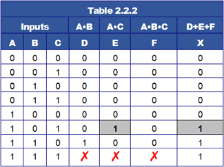
Compiling a truth table for Fig. 2.2.2 to check its operation produces Table 2.2.2. The output column X shows that the circuit in Fig. 2.2.2 does give the same outputs as Fig. 2.2.1. However, although a logic 1 at X is produced on the bottom row, where all three inputs (A•B•C) are logic 1, the third row up from the bottom of the table where A•C (shaded cells) also provides a logic 1 in column E and at output X.
Therefore it doesn’t matter whether columns D, E or F in the bottom row are at logic 1 or not. With the inputs at 111 the logic 1s on inputs A and C will still produce a logic 1 at E and therefore logic 1 at the output X. The bottom row for Columns D, E an F can therefore be marked with ✗ to indicate "Don’t Care", it doesn’t matter whether these cells are 1 or 0, column X will still be logic 1.
This means that column F (and the three input AND gate) are not needed, also the three input OR gate can be replaced by a two input OR gate.
Although the circuit shown in Fig. 2.2.2, designed from a Boolean equation derived directly from a truth table, does give the required output, the simpler (and cheaper) circuit shown in Fig. 2.2.1 does the job just as well. Using a truth table in this way will certainly give workable results and produce a working circuit, however it may not be the best circuit. In this case, the Boolean equation could be reduced and simplified by getting rid of the redundant A•B•C. The simplified circuit produced is then adequately described by the shorter Boolean equation:
X = (A•B) + (A•C)
This shows that although truth tables are an excellent method for analysing the operation of a digital circuit, they may not be the best design tool, when used on their own, for arriving at the simplest design. Simplifying circuit design using truth tables does require some practice in reading the truth table, although possible simplifications are still much easier to see in the truth table than by trying to visually analyse the circuit schematic diagram. However, with more complex circuits and more than two or three inputs, simplification using truth tables becomes a very laborious process, and therefore more prone to errors. For circuits using up to three or four inputs, better results can be obtained by the direct manipulation of the Boolean algebra equations obtained from a truth table.