
Module 3.2
How Transistors Are Made
- After studying this section, you should be able to:
- • Recognise alloy diffused & silicon planar transistors.
- • Recognise the advantages of silicon planar technology.
- • Describe the basic steps in planar transistor manufacture.
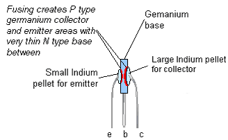
Fig 3.2.1 Germanium Alloy
Diffused Transistor
Alloy Diffused Transistors
Early bipolar junction transistors used a variety of methods to produce a current amplifier. Typically a thin wafer of Germanium was used for the base of the transistor. The emitter and collector were made by diffusing two pellets of Indium (a trivalent material, having three electrons in their valence shell) into either side of a wafer of N type base, as shown in Fig 3.2.1.

The fusion process causes the indium to diffuse into the germanium. As the two metals fuse together indium atoms (with 3 valence electrons) mix with the pure germanium atoms (with 4 valence electrons) creating P type material where the Indium atoms will appear to be short of one electron, and so will bond with only three instead of four neighbouring atoms. This creates a "hole" charge carrier at each Indium atom. Fusing is stopped just before the two P type regions meet. The result is an extremely thin layer of N type semiconductor (the BASE) sandwiched between two thicker P type layers, which form the other two terminals, the emitter and the collector. Notice that the P type region used for the collector is larger than the emitter region. This is because most of the heat generated within the transistor is generated at the base/collector junction. This junction therefore needs to be larger to dissipate this extra heat.
Alloy diffused transistors suffer from several drawbacks:
- 1. They have a poor frequency response due mainly to their large junction capacitances.
- 2. Their collector current increases as their temperature increases, making them susceptible to destruction due to thermal runaway.
- 3. They have relatively high leakage currents across the junctions.
- 4. They cannot withstand high voltages.
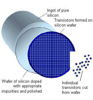
Fig 3.2.2 Multi Layer Construction
of a Silicon Planar Transistor.
Silicon Planar Transistors
The disadvantages of diffused alloy transistors was overcome in the 1950s by developing transistors that use silicon as the semiconductor material and the planar (layered) type of construction, illustrated in Figures 3.2.2 to 3.2.3 These transistors are built up as a series of very thin layers (or planes) of semiconductor material built up rather like a multi layer sandwich). Construction is more complex than the alloy diffusion technique, requiring many separate steps, depositing oxide layers on the silicon wafer and using photo lithographic techniques to etch away unwanted silicon areas. These steps are repeated with variations to build up the required patterns and layers to form either individual transistors or complete interconnected integrated circuits.
Although the many individual manufacturing steps are complex, from forming an ingot of very pure silicon, slicing it into wafers and forming the required components on the wafer, thousands of transistors can be made at the same time on a single wafer of silicon, this method of construction then becomes much cheaper and more reliable than the ‘one transistor at a time’ alloy diffusion method.
Once the transistors have been formed on the wafer, each one is tested automatically and any faulty transistors are marked with a spot of dye. The wafer is then cut up into the individual transistors and those marked as faulty are discarded.
The planar process is even more efficient when used to manufacture integrated circuits where numbers of interconnected transistors are fabricated on a single chip of silicon at the same time. The integrated circuits produced by this method may contain just a few interconnected transistors (Small Scale Integration or SSI), hundreds of transistors (Medium Scale Integration or MSI), thousands of transistors (Large Scale Integration or LSI), or devices such as microprocessors with millions of interconnected transistors (Very Large Scale Integration or VLSI). Figs. 3.2.2 to 3.2.4 illustrate the basic steps in the manufacturing process, assuming a wafer populated with single transistors.
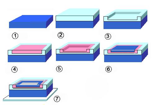
Fig 3.2.3 The Planar Construction Process.
Steps in Fig. 3.2.3
- 1. Layer 1 - Heavily doped N type Silicon.
- 2. Lightly doped N type silicon is deposited on top of layer 1 making a two layer collector. (see "How BJTs Work").
- 3. Part of the collector layer is etched away to form a depression for the P type base layer.
- 4. P type base layer is added.
- 5. Part of the base layer is etched away leaving a very thin base layer.
- 6. A heavily doped N type emitter layer is added.
- 7. Finally metal connectors are added allowing leads to be fixed after testing, and separating from the wafer.
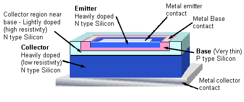
Fig 3.2.4 Completed Silicon Planar Transistor.