
Module 3.5
Current Gain
- After studying this section, you should be able to:
- Understand the use of common transistor characteristic graphs.
- • Transfer Characteristics.
- • Input & Output Characteristics.
- • Mutual Characteristics.
- In describing the operation of junction transistors.

A BJT is a current operated transistor, which means that the current flowing between emitter and collector of a transistor is much greater than that flowing between base and emitter. So a small base current is controlling the much larger collector/emitter current. The ratio of the two currents, ICE / IBE is constant, provided that the collector emitter voltage VCE is constant. Therefore, if the base current rises, so does collector current.
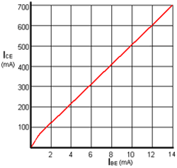
Fig. 3.5.1 Transfer Characteristic.
The BJT Transfer Characteristic
This ratio is the CURRENT GAIN of the transistor and is given the symbol hfe. A fairly low gain transistor might have a current gain of 20 to 50, while a high gain type may have a gain of 300 to 800 or more. The spread of values of hfe for any given transistor is quite large, even in transistors of the same type and batch. The graph of ICE / IBE shown in Fig. 3.5.1 is called the TRANSFER CHARACTERISTIC and the slope of the graph shows the hfe for that transistor
Characteristic curves (graphs) can be drawn to show other parameters of a transistor, and are used both to detail the performance of a particular device and as an aid to the design of amplifiers. The examples shown here are typical of BJTs, when used as voltage amplifiers.
The BJT Input Characteristic
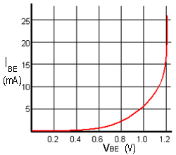
Fig. 3.5.2 Input Characteristic.
The INPUT CHARACTERISTIC (Fig. 3.5.2), a graph of base emitter current IBE against base emitter voltage VBE (IBE/VBE) shows the input CONDUCTANCE of the transistor. As conductance I / V is the reciprocal of RESISTANCE (V / I) this curve can be used to determine the input resistance of the transistor. The steepness of this particular curve when the VBE is above 1 volt shows that the input conductance is very high, and there is a large increase in current (in practice, usually enough to destroy the transistor!) for a very small increase in VBE. Therefore the input RESISTANCE must be low. Around 0.6 to 0.7 volts the graph curves, showing that the input resistance of a transistor varies, according to the amount of base current flowing, and below about 0.5 volts base current ceases.
The BJT Output Characteristic
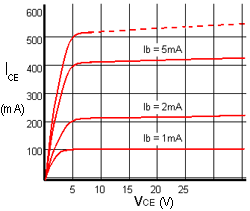
Fig. 3.5.3 Output Characteristic.
Fig. 3.5.3 shows the OUTPUT CHARACTERISTIC whose slope gives the value of output conductance (and by implication output resistance). The near horizontal parts of the graph lines show that a change in collector emitter voltage VCE has almost no effect on collector current in this region, just the effect to be expected if the transistor output had a large value resistor in series with it. Therefore the graph shows that the output resistance of the transistor is high.
These characteristic graphs show that, for a silicon transistor with an input applied between base and emitter, and output taken between collector and emitter (a method of connection called common emitter mode) one would expect;
- • Low input resistance (from the input characteristic).
- • Fairly high gain (from the transfer characteristic).
- • High output resistance (from the output characteristic).
The BJT Mutual Characteristic
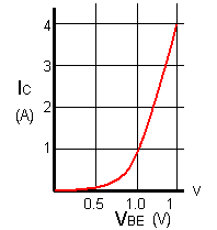
Fig. 3.5.4 Mutual Characteristic.
Fig. 3.5.4, the MUTUAL CHARACTERISTIC shows a graph of MUTUAL CONDUCTANCE IC/VBE and illustrates the change in collector current which takes place for a given change in base emitter voltage, (i.e. input signal voltage). This graph is for a typical silicon power transistor. Notice the large collector currents possible, and the nearly linear relationship between the input voltage and output current.
The characteristics described on this page are those relating to a typical power transistor connected in the ‘common emitter’ mode. This is one of three possible modes of connection for a transistor described in BJT Module 3.6. − Transistor Connections.
Note: In many transistors the currents will be much smaller than shown in these examples. For small signal amplifiers, base currents will be a few micro−amps rather than milliamps.