Google Ads
Module 2.2
Schottky Diodes
- After studying this section, you should be able to:
- • Understand construction methods used in Schottky Diodes.
- • Recognise advantages & disadvantages of Schottky Diodes.
- • Describe typical applications for Schottky Diodes.

Figure 2.2.1. Schottky Diode Circuit Symbol
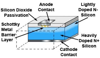
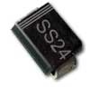
Figure 2.2.2. Small Signal Schottky Diode
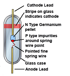
Figure 2.2.3. Germanium
Point Contact Diode
The Schottky Diode
Schottky diodes, also called Hot Carrier Diodes or Schottky Barrier Diodes use a metal/semiconductor junction instead of a P semiconductor/N semiconductor junction, a basic principle that dates back to the earliest ‘Cats Whisker’ diodes at the end of the 19th century. Although germanium diodes using the cats whisker or point contact principle illustrated in Fig. 2.2.3 fell into disuse by the late 20th century, a Metal/semiconductor junction is still used in Schottky diodes manufactured using silicon planar technology in place of the cats whisker, and can be manufactured with more reliable characteristics in both discrete component and integrated circuit form to provide the advantages of these early diodes in many modern circuits.
Low Junction Potential
The metal to silicon junction used in Schottky diodes provides several advantages (and some disadvantages) compared with a PN silicon diode. The P type region of the PN diode is replaced by a metal anode, usually gold, silver, platinum, tungsten, molybdenum or chromium. When the diode is formed during manufacture a small junction potential occurs between the metal anode and the N type silicon. Typically this will be about 0.15V to 0.3V depending on the metal used, and the difference between the energy levels of the electrons in the metal and the adjoining silicon, all of these metals produce a junction potential called the Schottky Barrier. Because this potential barrier is smaller than the 0.6V junction potential of a PN silicon junction, this makes Schottky diodes such as the BAT49 and the 1N5711 from ST Microelectronics very suitable for small signal radio frequency applications in circuits such as the RF mixer, modulator and demodulator stages in many radio communication systems, as well as high speed switching in digital logic circuits.
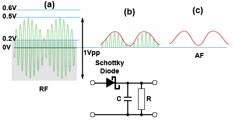
Figure 2.2.4. AM Demodulation Using a Schottky Diode
Basic AM Demodulation
Fig. 2.2.4 illustrates the advantage of using Schottky diodes for demodulating small amplitude AM waves. Amplitude Modulated signals are used in both broadcasts and communictaions as they can be transmitted over much longer distances using relatively low power transmitters than would be possible using VHF or UHF signals. When an AM signal is recieved its amplitude at the receiver may only be a few millivolts or even microvolts. This signal is greatly amplified by the receiver but may still be quite small (e.g. 1Vpp as shown in Fig. 2.2.4) when it is applied to the demodulator to recover the modulating signal. It would not therefore have sufficient amplitude (0.5V) to overcome the junction voltage of a silicon PN diode (0.6V), so no signal would be demodulated. Using a Schottky diode with a junction potential of only 0.2V however allows the demodulator to produce usable information from weaker signals than would be possible using a silicon PN diode.
The demodulation process involves applying the amplitude modulated signal to the Schottky diode, which only conducts when the positive half cycles of the RF are greater than 0.2V. (Fig. 2.2.4a) This produces an assymetrical RF signal that is applied to the capacitor C, which charges to nearly the peak value of each half cycle of the RF to produce a signal, (Fig. 2.2.4b) following the envelope shape of the RF signal, this is now an audio frequency waveform (shown in red)(Fig. 2.2.4c) that varies with the same shape as the audio signal originally used to modulate the RF. This demodulated audio signal is now amplified and used to drive the radio loudspeaker
High Speed Switching
A typical metal/N type Schottky junction works because when the junction is forward biased, the depth of the barrier decreases, allowing majority charge carriers (electrons) from the silicon to flood into the metal anode, where they are at a higher energy level than the electrons in the metal. Here they rapidly lose some of their energy and add to the free electrons in the metal, creating an electron flow from cathode to anode. When a reverse voltage is applied the junction however, the Schottky barrier level increases and the great majority of the electrons in the metal layer do not have a high enough energy level to re-cross the junction into the silicon, so only a very small leakage current flows, although the leakage current is greater than in a comparable PN diode.
Because, in a Schottky diode there is no exchanging and re-exchanging of holes and electrons across the junction, as happens in the PN diode, the switching speed is much faster. Schottky diodes therefore have a minimal Reverse Recovery Time (trr). Any delay in switching, which can be as low as 100 pico-seconds is mainly due to the capacitance of the junction, which especially in small signal switching types of Schottky diodes, as illustrated in Fig.2.2.2, is very small due to the small area of the junction. The junction capacitance is therefore typically less than 10pF, allowing some specialist types of Schottky diodes to operate at low voltages at frequencies in the GigaHertz and TeraHertz ranges.
Schottky Power Rectifiers
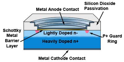
Figure 2.2.5. Schottky Rectifier Diode
In Schottky power rectifiers similar to that illustrated in Fig.2.2.5, this low junction potential is less important but does have the advantage that when the diode is conducting there is less power dissipated at the Schottky junction than in a comparable PN diode, so less heat is generated at the junction.
High Speed Switching Rectifiers
The main advantage in using Schottky diodes in power supplies is in its very fast switching speed. Many modern circuits use Switched Mode Power Supplies, which operate using square waves at high frequencies that need to be rectified at the power supply output. The fast switching speed of Schottky diodes such as the BYV44 from NXP or the BYV28 from Vishay are ideal for this purpose. However, the Schottky rectifier diode also has its drawbacks.
Schottky Reverse Current Limitations
Rectifier diodes are generally designed to handle large currents and large reverse voltages but the Schottky design is not as capable at either of these requirements as comparable PN junction diodes. Forward current generates heat at the diode junction and although the low junction potential of the Schottky design may generate less heat, the low junction potential of the Schottky depends on a very thin (the thinner the junction the lower the potential) metal layer at the junction. A thinner layer also means that the reverse leakage current of the diode will be greater. This can be seen from a comparison of typical PN and Schottky characteristic curves (not to scale) shown in Fig. 2.2.6. Also, although the Schottky junction may be considered to generate less heat per Watt than the PN junction, in order to keep its reverse leakage current within acceptable limits, the maximum junction temperature must be kept below typically 125°C to 175°C (depending on type) compared with 200°C or more for a PN diode.
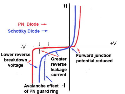
Figure 2.2.6. Schottky & PN Characteristics
Compared
Over Voltage Protection
If the reverse leakage current is not carefully controlled and the diode also protected against sudden spikes in voltage, it is possible that the current may become large enough (even momentarily) to take the reverse current into the reverse breakdown region and destroy the diode. To prevent this, it is common in Schottky rectifiers to include a Guard Ring round the junction area, this consists of a ring of heavily doped P+ type silicon embedded into the N- type cathode region, in effect forming a reverse biased PN junction within the Schottky diode structure, as can be seen in Fig. 2.2.5. Because the guard ring is heavily doped it behaves rather like a Zener diode with pronounced avalanche characteristics, i.e. it will suddenly conduct heavily in its reverse current mode at a precise reverse voltage. This point is designed to be at a lower voltage than the breakdown voltage of the Schottky junction, therefore the Schottky diode is protected as the current taken by the PN junction will be sufficient to prevent the reverse voltage rising above safe limits.
For any circuit design it is important to carefully consider the advantages and disadvantages of both Schottky and PN Junction diodes to ensure that the chosen components will perform both efficiently and reliably. There is no simple answer to which of these types of diode is most suited to a particular purpose. It is a matter of selecting a diode whose individual parameters match the required purpose. Schottky rectifier diodes may be preferable for switching speed and efficiency, and PN diodes better for higher current and voltage designs. But the final choice depends on the characteristics of the individual components.