
Module 4.3
Enhancement Mode MOSFETs.
- Section 4.3 The Enhancement Mode MOSFET.
- • The IGFET (Insulated Gate FET).
- • MOSFET(IGFET) Construction.
- • MOSFET(IGFET) Operation.
- • MOSFET (IGFET) Circuit Symbols.
- • Handling Precautions for MOSFETS
The Insulated Gate FET (IGFET).
The Metal Oxide Silicon FET (MOSFET) or Metal Oxide Silicon Transistor (M.O.S.T.) has an even higher input resistance (typically 1012 to 1015 ohms) than that of the JFET. In the MOSFET device the gate is completely insulated from the rest of the transistor by a very thin layer of metal oxide (Silicon dioxide SiO2). Hence the general name applied to any device of this type, is the IGFET or Insulated Gate FET.
Planar Technology.
There are several ways in which an insulated gate transistor may be constructed. All the methods used however, make use of planar technology in which the various parts of the device are laid down as planes or layers on the upper surface of a "SUBSTRATE" in a similar way to that shown on the Planar Transistors page in the BJT section.
The layers are laid down one by one, by diffusing various semiconductor materials with suitable doping levels, as well as layers of insulation into the surface of the device, under carefully controlled conditions at high temperatures. Parts of a layer may be removed by etching, using photographic masks to make the required pattern of the electrodes etc. before the next layer is added. The insulating layers are made by laying down very thin layers of silicon dioxide and conductors are created by evaporating a metal, such as aluminium on to the surface. The transistors produced in this way have a much higher quality than is possible using other methods, and many transistors can be produced at one time on a single slice of silicon, before the silicon slice is cut up into individual transistors or integrated circuits.
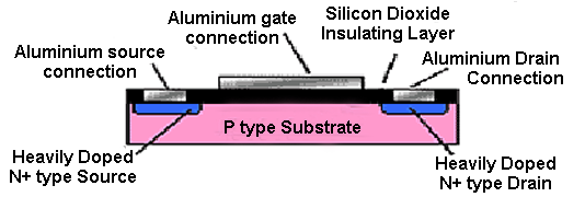
Fig. 4.3.1 N Channel Enhancement Mode
MOSFET Construction
MOSFET (IGFET) Construction.
The basic construction of a MOSFET is shown in Fig. 4.3.1. A body or substrate of P type silicon is used, then two heavily doped N type regions are diffused into the upper surface, to form a pair of closely spaced strips.
A very thin (about 10-4 mm) layer of silicon dioxide is then evaporated onto the top surface forming an insulating layer. Parts of this layer are then etched away above the N+ type regions using a photographic mask to leave these regions uncovered. On top of the insulating layer, between the two N type regions, a layer of aluminium is deposited. This acts as the GATE electrode. Metal contacts are also deposited on the N+ type regions, which act as the SOURCE and DRAIN connectors.
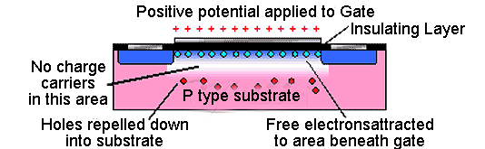
Fig. 4.3.2 N-Channel Enhancement Mode
MOSFET Operation.
MOSFET (IGFET) Operation.
The gate has a voltage applied to it that makes it positive with respect to the source. This causes holes in the P type layer close to the silicon dioxide layer beneath the gate to be repelled down into the P type substrate, and at the same time this positive potential on the gate attracts free electrons from the surrounding substrate material. These free electrons form a thin layer of charge carriers beneath the gate electrode (they can't reach the gate because of the insulating silicon dioxide layer) bridging the gap between the heavily doped source and drain areas. This layer is sometimes called an "inversion layer" because applying the gate voltage has caused the P type material immediately under the gate to firstly become "intrinsic" (with hardly any charge carriers) and then an N type layer within the P type substrate.
Any further increase in the gate voltage attracts more charge carriers into the inversion layer, so reducing its resistance, and increasing current flow between source and drain. Reducing the gate source voltage reduces current flow. When the power is switched off, the area beneath the gate reverts to P type once more.
As well as the type described above, devices having N type substrates and P type (inversion layer) channels are also available. Operation is identical, but of course the polarity of the gate voltage is reversed.
This method of operation is called "ENHANCEMENT MODE" as the application of gate source voltage makes a conducting channel "grow"; therefore it enhances the channel. Other devices are available in which the application of a bias voltage reduces or "depletes" the conducting channel. These are described on the Depletion Mode MOSFET page.
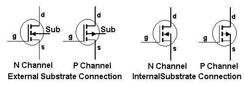
Fig. 4.3.3 Circuit Symbols for Enhancement Mode MOSFETs (IGFETs)
Handling Precautions.
In operation, although the gate has a voltage applied to it, no gate current flows because of the silicon dioxide layer beneath the gate terminal. One well known problem exists regarding this layer however. Although silicon dioxide is an excellent insulator, the layer used on a MOSFET is extremely thin, and therefore can be permanently damaged if a high voltage is applied across it. It will break down just as any other insulator will. Because it is so very thin, it does not need very high voltages to cause total breakdown, and as the gate has such a very high resistance, any voltage present will not be reduced by current flow.
Therefore voltages due to static electricity, which are present all the time in almost any environment, and may reach several thousand volts if no current is drawn to discharge them, present a threat to the insulating layer. For this reason it is wise to transport FETs in special conductive packaging so that no voltage can build up between any of the terminals of the device. Once the transistor is connected into a circuit, the components of the circuit should afford sufficient protection by forming conducting paths around the device, so preventing the build up of high static voltages. In most modern devices special protection diodes are built in to the device to give some protection against static damage. This protection is limited however, and manufacturers handling instructions should be studied before handling any MOS device.
An informative Data Sheet "Handling Instructions and Protection against Electrostatic Discharges" is produced by the Microsemi Corporation and is available via our Links page.