
Module 4.6
MOSFET Switches
- After studying this section, you should be able to:
- Understand the operation of Power MOSFET switches.
- Recognise important characteristics of Power MOSFETs.
- Choose appropriate Power MOSFETs for switching DC current.
- Describe typical driver circuits for power MOSFETs in switching and controlling high current loads.
- Recognise typical safety measures to prevent damage due to over heating, over voltage or over current.
Building MOSFET Switches.
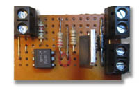
Fig. 4.6.2 The MOSFET Switch

Fig. 4.6.3 PWM+Logic
Signal Source
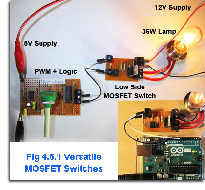
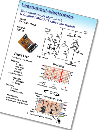
To test the calculations made in Module 4.5, the circuit shown in Fig. 4.6.2 was built on strip board (proto-board). Only a few components are needed and the circuit also incorporates an opto-isolator to isolate any logic input circuit from the high current high voltage output that the switch may be controlling.
The MOSFET switch circuit load in this case is a 12V 36Watt automotive headlamp bulb and the input to the MOSFET switch will be a pulse width modulated, logic level signal. This may be supplied by any 5V compatible logic circuit producing a PWM signal at a frequency in the high audio frequency range. In initial tests the N Channel MOSFET Low Side switch was connected to a Pulse Width Modulated (PWM) + Logic circuit based on a modified version of the single 555 timer design (Fig. 4.4.8) in the Learnabout-Electronics Oscillators section where a description of its operation can be found. For these tests, a Schmitt inverter was added to ensure fast rise and fall times to the resulting PWM output signal. You can download full construction details for the PWM circuit here.
AAlternatively the variable PWM input signal could be obtained from any circuit having a 5V logic output, such as the Arduino as shown in Fig 4.6.9, in this case running the simple PWM sketch, which continually dims and brightens the lamp.
The circuit diagram for the switch is shown in Fig. 4.6.5 and the layout for initial tests is in Fig. 4.6.1.
Fig 4.6.4 The N Channel Low Side Switch
Pulse Width Modulation Sources
Two outputs are available from the PWM circuit, which are the actual PWM signal and an inverted version. Either can be applied to the input terminals of the MOSFET circuit. For testing, the output of the MOSFET switch was connected to a 36 Watt load (an automotive headlamp bulb) connected between the 12V lamp supply and the Drain terminal of the MOSFET Switch as shown in Fig 4.6.5. This represents the 3A maximum load the circuit is designed for, as 3A is also a common maximum current available from bench power supplies.
The PWM input signal can also be obtained from any circuit having a 5V logic output, such as the Arduino as shown in Fig 4.6.8, in this case running the simple PWM sketch, which continually dims and brightens the lamp.
The operation of the Pulse Width Modulator circuit is based on the 555 circuit described in Oscillators Module 4.4. For use as a MOSFET driver, the circuit has been slightly modified to increase its frequency of operation, as when it is used for driving loads such as DC Brushed motors the frequency of operation needs to be high enough to avoid causing an audible whine, as the inductive nature of the motor can make it operate as a loudspeaker at low frequencies. The action of the opto-isolator is also described in Semiconductors Module 5.2.
A MOSFET Switch Circuit
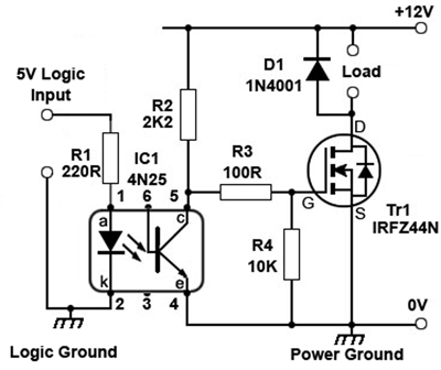
Fig. 4.6.5 The MOSFET Switch With Isolated Input
The opto-isolator (IC1) and its two resistors R1 and R2 are not absolutely essential to the operation of the MOSFET but are highly desirable because the complete circuit makes a very useful self contained switch, suitable for interfacing many low voltage, low current electronics projects to higher voltage/current peripherals. IC1 performs two functions; it isolates any external driving circuit from the MOSFET and also increases the amplitude of a 5V logic signal sufficiently to drive a standard (i.e. not logic input version) MOSFET without the need for an additional amplifier. The purpose of R3 is to prevent or dampen any ringing that may be caused by the combination of the gate capacitance and the inductance of any wiring, especially in drive circuits working at high frequencies, where this is more important when driving higher frequency circuits such as switched mode power supplies. A Typical value for R3 would be 100Ω or less as higher values can slow down switching.
It is Essential when switching MOSFETs that the switching time between the off and on states is kept as short as possible. When the MOSFET is Fully switched on (saturated) The Drain-Source Voltage is close to zero, so although there may be a large current flowing, the power dissipated (I2R) is very small. When the MOSFET is switched off there will be a large voltage between Drain and Source but practically no current is flowing so again the power dissipated in the MOSFET is practically zero Watts. However during the changes between on and off, both voltage and current will be considerable and so large amounts of power will be dissipated for a very short time. Therefore the quicker the MOSFET can be switched on or off the less power will be dissipated. The total power dissipated during each operating cycle will be approximately the sum of the dissipation during each of the off-to-on and on-to-off periods.
R4 ensures that as the MOSFET switches off when the positive gate drive signal is removed, the gate capacitance is discharged immediately to zero volts rather than remaining close to the switch on level, so reducing the probability of random switch on of the MOSFET. D1 is connected across the load terminals to prevent damage to the MOSFET due to back emf when used with inductive loads.
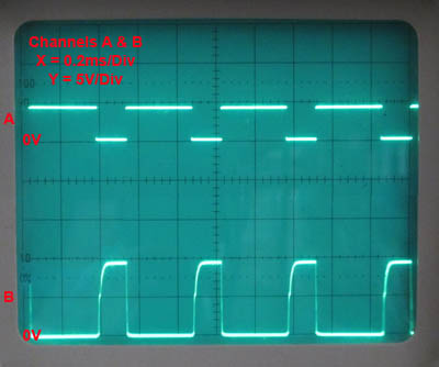
Fig. 4.6.6 4N25 Opto-isolator Waveforms
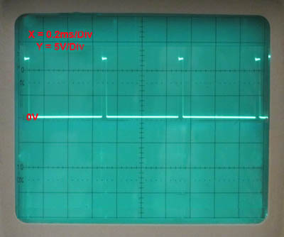
Fig. 4.6.7a Drain Waveform at Minimum Power
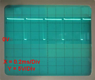
Fig. 4.6.7b Drain Waveform at Maximum Power
Looking at the switching action of the MOSFET, it can be seen from the waveforms in Figs. 4.6.6 and 4.6.7 a and b. Notice in Fig. 4.6.6 that there is some curvature to the rising voltage in waveform B (the opto-isolator output), which tends to slow down the switching. This is due to the relatively slow switch on time (compared with the operating frequency) of the opto-isolator. However, looking at the drain waveforms in Figs. 4.6.7 a and b this has not adversely affected the switch on time of the MOSFET as the curvature in the opto-isolator output waveform is mainly in the upper voltage levels of the 10Vpp gate signal, after the MOSFET has already switched on. Note that the 4N25 opto-isolator is not rated as particularly fast; there are a number of faster devices, which use opto diodes instead of opto transistors as the output component, however they do tend to cost more and are more likely to be used in higher frequency systems.
Temperature Tests
On testing the temperature rise for the whole circuit used in Figs. 4.6.8 and 4.6.9 it was found that although the calculations suggested a temperature rise only very slightly above 25°C would be achieved, the completed circuit shown in Fig. 4.6.9 actually ran at a maximum temperature of around 28°. Higher than the calculations suggest but still well within safe limits when using a 3A motor as the load. With the circuit connected to the 36Watt lamp however, as shown in Fig. 4.6.8, the temperature rise was considerably higher, rising to around 37°C, this appeared to be due in some part to the lamp (very hot) being so close to the MOSFET and therefore raising the ambient temperature. The MOSFET temperature dropped back, close to 29° when a small sponge shield was placed between the lamp and the MOSFET.
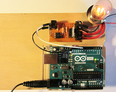
Fig. 4.6.8 Arduino Driving a 36 Watt Lamp.
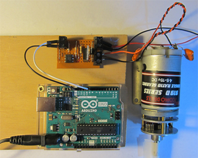
Fig. 4.6.9 Arduino & a 3A DC Motor.
The switch therefore worked well with both resistive (12V lamp) and inductive (brushed DC motor) loads upto 3A when driven from a 12V supply with an input from a 5V logic source. The input signal was provided by either a simple pulse width modulator circuit or the Arduino.
The circuit also performed well with the MOSFET replaced by a 039N04L logic level MOSFET. In this case it would not be strictly necessary to use the 4N25 opto-isolator to boost the logic input level to the 10Vpp needed by the IRFZ44N, but then the input circuit would be exposed to any fault condition in the MOSFET circuit. The extra expense in using an opto-isolator compared with a wrecked Arduino is therefore justified.
High Side and Low Side Switching
The MOSFET in the above example is placed between the load and ground, this method of operation is therefore called Low Side Switching and is a simple and much used method of using MOSFET switches. However there are some applications where this may not be suitable, as when the load requires a ground connection in common with other load devices. Also when the MOSFET is 'off' and current through the load ceases, the voltage at Point X in Fig. 4.6.11a will be at the supply voltage. Whilst this may not be a problem at low voltages, MOSFETs can be used to switch high voltage circuits where having a high voltage present on an apparently inactive circuit can be a safety problem by creating a shock hazard. To eliminate either of these problems, High Side Switching can be used, as shown in Fig. 4.6.11b. where, when the MOSFET switches off the voltage across the load (and at point X) will be at zero volts, (providing that the MOSFET does not develop a short circuit fault).
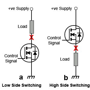
Fig. 4.6.11 Low and High Side Switching
Low side switching is simple to implement using N channel Power MOSFETs but High Side Switching raises some difficulties. The main problem that must be overcome is that the gate voltage (VGS) on an N channel MOSFET must be more positive than the Source voltage in order to switch the MOSFET on. While the MOSFET is off in a high side circuit the Source voltage will be virtually zero volts so the Gate could switch the MOSFET on, but once it is on, the Source voltage will be almost the same as the Drain voltage due to the very low resistance of the conducting MOSFET. As the supply voltage (and now also the source voltage) is likely to be the highest voltage in the circuit, the Gate voltage cannot be made higher than the Source voltage and control is lost.
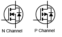
Fig. 4.6.12 N & P Channel
Enhancement MOSFETs
The High Side MOSFET Switch
To make High Side Switching possible there are a number of methods that can be used. The simplest of these is to replace the N channel MOSFET with a P channel type. The circuit symbols for each are shown in Fig. 4.6.12. The only difference in these symbols is the direction of the arrow indicating the channel; in the P channel MOSFET the arrow now points away from the P type channel.
However the connection of the P channel MOSFET compared with the N channel is reversed, The P channel source is connected to the positive supply and the gate must now be connected to a lower voltage that the source in order for the MOSFET to switch on. The drain is now connected to the more positive side of the load, and the load's negative terminal is connected to ground.
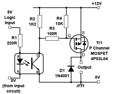
Fig. 4.6.13 P Channel High Side Switch

A circuit for a typical high side switch using a P channel MOSFET is shown in Fig. 4.6.13. Notice the similarities and differences between Figs. 4.6.13 and 4.6.5. Firsly in Fig.4.6.13 the resistor R4 whose purpose is to discharge any remaining potential on the gate at switch off is now connected to the positive supply rail instead of to ground. This indicates that the gate potential, when switched on will be more negative than supply providing a negative value of VGS.
Fig. 4.6.13 also uses a different opto-isolator, a PC817 instead of the 4N25 in Fig. 4.6.5. This is not an important difference as a number of similar isolators could be used, it just needs to have a reasonable 12Vpp output waveform to switch the MOSFET Gate. The MOSFET used in the this high side switch is a logic level 4P03L04 from Infineon and as it only needs its gate to be 4.5V lower than the 12V supply, the 12Vpp waveform applied to its gate easily switches the MOSFET on or off.
The P Channel High Side Switch therefore solves the problem of using an N Channel MOSFET for high side switching; however this 'cure' can also have some side effects. P channel MOSFETs generally have a higher RDSon compared to N type MOSFETs having a similar internal chip size. This means that during the time when the MOSFET is on, a P type MOSFET will produce more heat than a similar N type device. This is especially relevant in high current circuits. However as this module restricts itself to relatively low power circuits the difference in RDSon values is less of a concern. For example the P channel 4P03L04 has an RDSon value of 4.4mΩ whereas the N channel IRFZ44N has a RDSon value of 17.5mmΩ. Despite this the section below describes a method for using an N channel MOSFET in a high side switch circuit.
The N Channel High Side Switch
The main problem in using an N channel MOSFET in a high side switch is that in order for the MOSFET to switch on, once it has been switched off is that the voltage on the gate terminal of the MOSFET must be made higher than the source voltage, which, as the MOSFET is "off" will be at supply voltage Vcc. In order to do this the gate voltage must be 'level shifted' in some way. This technique commonly goes under the name of 'Bootstrapping' (i.e. the mythical abbility to lift oneself up simply by pulling upwards on your boot straps) - apart from the impossibility of this task, Bootstrapping is not the most useful name, as there are several techniques used in other non-related circuits that use the same name, generally meaning to lift some value up to a higher than normal level.
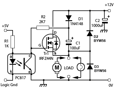
Fig. 4.6.14 N Channel High Side Switch
In this case the "off" voltage (the lowest voltage of the wavaveform) at the MOSFET gate needs to be lifted up to at least as high as the supply voltage. For example if a logic level MOSFET is used, the minimum gate voltage would be equal to the supply voltage (5V) and the peak gate voltage would need to be 5V higher than the supply voltage Vcc.
With non-logic level MOSFETs the minimum gate voltage will need to be at about the supply voltage (e.g.12V) and the peak voltage approximately double the voltage of Vcc. The purpose of bootstrapping is to achieve these increases without an external supply.
This only requires a few extra components, but the system only works for MOSFET circuits that are continuously switched on and off (such as PWM circuits). Circuits that are turned on for long periods require different techniques.
How the Bootstrap Circuit Works
When the output transistor of the opto-coupler is switched on, its collector terminal and the MOSFET gate voltage is pulled down to 0V; The MOSFET is switched off and with the Drain voltage at Vcc (12V), the capacitor C1 charges via the diode D1 to almost Vcc (12V). When the opto-isolator output transistor switches off again, its collector voltage and the MOSFET gate rise to Vcc (12V) and the MOSFET turns on. This however, also makes the Source voltage rise to 12V (which without bootstrapping would instantly switch the MOSFET off again as source and gate would be the same voltage). However as C1 is now charged up to 12V, its negative terminal will be at 12V but its positive terminal will now be 12V + 12V = 24V, (pulling the gate voltage up by its bootstraps!) and also reverse biasing the diode D1. So with the gate terminal of the MOSFET now at 24V the MOSFET stays switched on, Eventually of course the capacitor would discharge and the gate voltage reduce towards a level that would cause the MOSFET to turn off again, except for the fact that the input signal is switching on and off continually. So provided that the 'off' time is long enough for the capacitor to recharge during each cycle and the 'on' time is not long enough for C1 to discharge, (which would be a comparatively very long time due to the MOSFET's very high gate resistance) the MOSFET continues to work.