
Module 5.1
Clock Circuits
- After studying this section, you should be able to:
- Understand the need for clock generators.
- Recognise clock generator circuits.
- • RC clocks.
- • Crystal controlled clocks.
- Recognise clock generator circuits.
Clocks and Timing Signals
Most sequential logic circuits are driven by a clock oscillator. This usually consists of an astable circuit producing regular pulses that should ideally:
1. Be constant in frequency
Many clock oscillators use a crystal to control the frequency. Because crystal oscillators generate normally high frequencies, where lower frequencies are required the original oscillator frequency is divided down from a very high frequency to a lower one using counter circuits.
2. Have fast rising and falling edges to its pulses.
It is the edges of the pulses that are important in timing the operation of many sequential circuits, the rise and fall times are usually be less than 100ns. The outputs of clock circuits will typically have to drive more gates than any other output in a given system. To prevent this load distorting the clock signal, it is usual for clock oscillator outputs to be fed via a buffer amplifier.
3. Have the correct logic levels
The signals produced by the clock circuits must have appropriate the logic levels for the circuits being supplied.
Simple Clock Oscillator

Fig. 5.1.1 Simple Schmitt Inverter Clock Oscillator
Fig 5.1.1 is probably the simplest oscillator possible, having only three components. Notice that the gate is a Schmitt inverter. This device has an extremely fast change over between logic states. Also the level at which it responds to an input change from 0 to 1 (Vt+) is higher than the level at which it changes from 1 to 0 (Vt-). The operation of the circuit is as follows.
Suppose the gate input is at logic 0, because the gate is an inverter, the output must be at logic 1, and C will therefore charge up via R from the output. This will happen with the normal CR charging curve. Once Vt+ is reached at the gate input, the gate output will rapidly switch to 0. The resistor is now connected effectively between the positive plate of C and zero volts. Thus the capacitor now discharges via R until the gate input voltage reduces to Vt- when the output will change to logic 1 once more, starting the charging and discharging cycle over again.

Fig. 5.1.2 Typical Basic Schmitt Oscillator Output
This Schmitt RC oscillator can produce a pulse waveform with an excellent wave shape and very fast rise and fall times. The mark to space ratio, as shown in Fig 5.1.2 is approximately 1:3.
The frequency of oscillation depends on the time constant of R and C, but is also affected by the characteristics of the logic family used. For the 74HC14 the frequency (ƒ)is calculated by:

When using the 74HCT14 the 0.8 correction factor is replaced by 0.67, however either of these formulae will give an approximate frequency. Whichever logic family is used, the frequency will vary with changes in supply voltage. Although this basic oscillator gives an excellent performance in many simple applications, if a stable frequency is an important factor in the choice of clock oscillator, there are of course better options.
Crystal Controlled Clock Oscillator

Fig. 5.1.3 Crystal Controlled Clock Oscillator
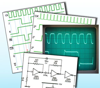
Fig. 5.1.3 uses three gates from a 74HCT04 IC, and a crystal to provide an accurate frequency of oscillation. Here, the oscillator is running at 3.276MHz but this can be reduced by dividing the output frequency down to a lower value by dividing it by 2 a number of times using a series of flip-flops.
The top waveform in Fig 5.1.4 shows the clock signal generated by Fig 5.1.3, and beneath it is the clock signal frequency divided by 4 after passing it through two flip-flops. Notice that after passing the signal through flip-flops, as well as being reduced in frequency, the wave shape is considerably squarer and now has a 1:1 mark to space ratio.

Fig. 5.1.4 Clock Frequency Divided by 4
The 555 Timer Clock Generator
Another option in circuits not requiring very high frequency clock signals is to use the 555 Timer in astable mode as a clock generator. This IC is able to produce good quality pulse or square wave signals over a wide range of frequencies, lower than those possible with crystal oscillators, also the frequency stability will not be as good as with crystal controlled oscillators. Several oscillator design options are discussed in Oscillators Module 4.4
Two Phase Clock Signals
Some older microprocessor systems required two-phase clock signals which, provided that the source clock signal operated at twice the frequency required by the microprocessor, saved processing time as the microprocessor was able to carry out two actions per clock cycle instead of one.
Producing a Two-Phase Clock Signal
If a clock signal with a 1:1 mark space ratio is used, two non-overlapping clock pulses can be created, using the circuit shown in Fig 5.1.5. These signals are usually called Φ01 and Φ02 (Φ the Greek letter Phi is used to indicate phase).

Fig. 5.1.5 Two-Phase Clock Generator
In Fig 5.1.5 a single clock signal having a 1:1 mark to space ratio is fed into a JK flip-flop working in toggle mode. This is achieved by making both J and K logic 1. The active low PR and CLR inputs take no part in the operation of this circuit so are also tied to logic 1. In toggle mode the Q output of the JK flip-flop inverts the logic levels at Q and Q at every falling edge of the clock(CK) input, also Q and Q output always remaing at opposite logic states.
Each of the NAND gates will then produce a logic 0 output whenever both its inputs are at logic 1. The NAND gate producing Φ01 therefore creates a logic 0 pulse whenever CK and Q are at logic 1, and the NAND gate producing Φ02 creates a logic 0 pulse whenever CK and Q are at logic 1.

Fig. 5.1.6 Two-Phase Clock Signal
Fig. 5.1.6 illustrates the operation of Fig 5.1.5. Each of the NAND gates will produce a logic 0 output whenever both its inputs are at logic 1. The NAND gate producing Φ01 therefore creates a logic 0 pulse whenever CK and Q are at logic 1, and the NAND gate producing Φ02 creates a logic 0 pulse whenever CK and Q are at logic 1. Typical output waveforms are illustrated in Fig. 5.1.7.
If positive going clock pulses are required, the outputs from the NAND gates may be inverted using Schmitt inverters, which will also help to sharpen the rise and fall times of the clock waveforms.
Distributing Clock Signals
For more demanding applications there are very many specialised clock oscillator ICs available that are typically optimised for a particular range of applications, such as computer hardware, wireless communications, automotive or medical applications etc.
Clock Fan-out
Whatever circuit is used to generate a clock signal, it is important that its output has sufficient fan-out capability to drive the necessary number of ICs requiring a clock input, and that the clock signal is not degraded in amplitude, speed of its rise and fall times or accuracy of its frequency. Also, by maintaining fast rise and fall times, ringing on the waveform can become a problem. The waveform should be kept as close as possible to a perfect square wave shape.

Fig. 5.1.7 Two Phase Clock Waveforms
Circuit Capacitance
Because the clock must feed many gates, the small capacitance of each of these gates will add, to become an appreciable capacitance, which loads the clock output tending to slow the rise and fall time of the clock signal. To avoid this, the clock output must have a low enough impedance to rapidly charge and discharge any natural capacitance in the circuit. The usual way to achieve this is to feed the clock signal via a special clock buffer gate, which will have the necessary low output impedance and a large fan out factor. Schmitt trigger gates may also be used to restore the shape and integrity of clock signals before they are applied to gates in different parts of the circuit.
Cross-talk
Where the clock signal has to be distributed around large circuits, there is a greater chance of introducing noise, and possible ‘cross-talk’ where data in one conductor is radiated into another nearby conductor. Problems such as this will increase the likelihood of ‘skew’ errors, i.e. clock signals arriving at different parts of the circuit at slightly different times, due to small changes in the phase of some of the distributed clock signals. Miniaturisation brought about by surface mount technology can help minimise these problems. Also when clock signals need to be sent from one system to another over an external wired or wireless link it is common to use one of the several ECL or LVDS logic families with their differential outputs to minimise interference, and there are many application specific ICs (ASICS) using these technologies for high frequency clock distribution.