Module 5.5
CMOS Flip-flops
- After studying this section, you should be able to:
- Describe the differences between TTL and CMOS flip-flop circuits and can:
- • Recognise a transmission gate (bi-lateral switch).
- • Describe the action of a transmission gate.
- • Describe the action of a bi-stable flip-flop using transmission gates.
- Understand how CMOS circuits are used in flip-flop ICs.
- • CMOS D Type flip-flops.
- • CMOS JK flip-flops.
- Use circuit software to simulate CMOS flip-flops.
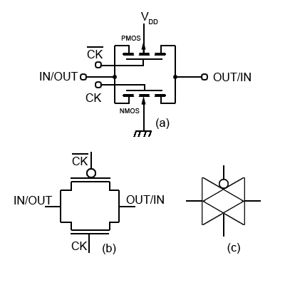
Fig. 5.5.1 The CMOS Transmission Gate
CMOS Transmission Gates
The flip-flops described so far in this module have been based on TTL technology, however many modern devices such as the 74HC and 74HCT series are CMOS ICs, which have radically different internal structures. The flip flops in CMOS ICs depend on a different type of gate, called a ‘Transmission Gate’ or ‘Bi-lateral Switch’, which make it possible to construct bi-stable flip-flops using less space within the IC, and have simpler structures than those used in TTL ICs.
Fig. 5.5.1(a) illustrates the basic structure of a transmission gate, which in some ways operates in a similar way to an electro-mechanical relay switch, except that it is much faster and very much smaller.
Like a relay, once it is energised, information can flow through the switch in either direction, therefore the signal terminals are dual purpose and can be labelled in/out and out/in. In a transmission gate this is because the signal path is via two metal oxide silicon (MOS) transistors, one of which is PMOS and the other is NMOS, connected in parallel. Signals, either digital or analogue, can pass between source and drain of these transistors in either direction when they are made to conduct by placing an appropriate voltage on the gate terminal of each transistor.
The switching signal in digital circuits is provided by the clock pulses CK and CK. When the CK pulse is applied to the gate of the NMOS transistor and the CK to the PMOS transistor gate, the signal channel between the input and output terminal will conduct, and have a typical resistance of about 125O. In the absence of these pulse voltages however, or if they are reversed, with CK applied to the PMOS gate and CK applied to the NMOS gate, the conduction channel will exhibit an extremely high impedance (1 x 10¹²Ω), virtually open circuit.
CMOS Flip-flop
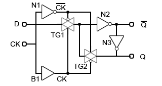
Fig 5.5.2 shows a basic circuit for a single flip-flop, which operates as a level triggered D Type flip-flop. Apart from the NOT gate (N1) and the buffer (B1) controlling the CK input, the basic flip-flop uses only two NOT gates (N2 and N3) and two transmission gates (TG1 and TG2).
CMOS Flip-flop Operation
The inverter N1 and the Buffer B1 create clock pulses CK and inverted clock pulsesCK, which (because N1 and B1 have identical propagation delays), will exactly coincide in time when applied to the transmission gates of the flip-flop circuit.
Initially, assuming that the CK and D are both at logic 0, CK will be at logic 1, so transmission gate TG1 will be in its high impedance state, preventing D from having any effect upon the flip-flop.
When CK is logic 1 and CK is logic 0, TG1 will conduct and the logic 0 from D will be inverted by N2, so the output Qwill become logic 1. The logic 1 at Q will be inverted by N3 to become logic 0 at the Q output.
The logic 1 at Q will not affect the logic 0 at the input to N2 as TG2, connected in opposite polarity to the CK and CK clock signals will be turned off. This condition will remain stable irrespective of any further clock pulses being applied, as whenever TG1 is turned on, TG2 is turned off.
If input D is now changed to logic 1 between the occurrence of clock pulses, the rising edge of the first clock pulse after the change at D will turn on TG1, transmitting the logic 1 from D to the input of N2, causing Qto change to logic 1 and (via N3) Q to change to logic 0.
Whilst the CK input is high, any changes at D will be transmitted via TG1 and N2 to the outputs, indicating that the flip-flop is level triggered, but the moment the falling edge of the clock pulse occurs, TG1 will turn off and TG2 will turn on, isolating N1 and N2 from any further changes at the D input and leaving the output of N3 connected via TG2 to the input of N1.
As both these points will be at the same logic state (the logic state existing at D before the falling edge of the CK pulse) the flip-flop outputs will remain in a stable mode until the next clock pulse, when Q will take up the same state as input D once more.
Practical CMOS Flip-flop Circuits
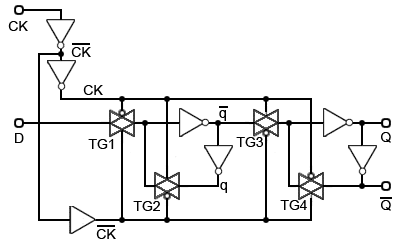
Fig. 5.5.3 illustrates a CMOS D Type Positive Edge Triggered Master Slave Flip-flop. Notice that each pair of transmission gates TG1/ TG2 in the master flip flop, and TG3/TG4 in the slave flip-flop are connected to the clock lines in the opposite sense to each other, so that as soon as the master flip-flop accepts data from D at the rising edge of the CK pulse, the slave flip-flop is inhibited, preventing any further change at the outputs, effectively giving positive edge, rather than level triggering.
Buffered Inputs and Outputs
Buffered inputs and outputs, together with input static protection are common to most sequential ICs, but have been omitted from the schematic diagrams in this module for clarity of operation. The buffer gates and protection circuits used can be found in data sheets for individual IC designs that can be downloaded from the links at the end of this module.
CMOS D Type Flip-flop with SET and RESET
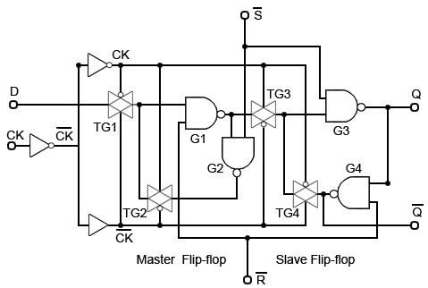
Fig. 5.5.4 shows how a CMOS D Type master slave flip-flop may be modified to include Sand R inputs. In this version, NAND gates have replaced the inverters used in the master and slave flip-flops in Fig 5.5.3.
When logic 0 is applied to the S input, G3 output (and Q) is set to logic 1, (as a NAND gate output can only be logic 0 when all of its inputs are at logic 1).
Making S logic 0 also disables both the master and slave flip-flops by forcing both G3 and G2 outputs to logic 1. Therefore neither the clock nor the D inputs will have any effect on the Q and Qoutputs whilst S is low.
The RESET input (R) works in the same way, by forcing the NAND gates G1 and G4 to have logic 1 outputs.
The CMOS JK Flip-flop
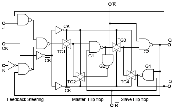
Converting the D Type flip-flop shown in Fig. 5.5.4 into the fully featured JK Flip-flop shown in Fig 5.5.5 is a simple matter of adding positive feedback lines from the Q and Qoutputs to the two J and K input gates of the feedback steering circuit, which is simply a modified version of the basic data select circuit described in Digital Electronics Module 4.2.
JK Flip-flop ICs.
74HC107 Dual Negative Edge Triggered JK Flip-flop with RESET from NXP
74HC109 Dual Positive Edge Triggered JK Flip-flop with SET and RESET from NXP
74HC112 Dual Negative Edge Triggered JK Flip-flop with SET and RESET from NXP
HEF4027 Dual Positive Edge Triggered JK Flip-flop with SET and RESET from NXP


