
Google Ads
Module 6.2
SCRs in AC Circuits
- After studying this section, you should be able to:
- Describe methods for AC power control using SCRs
- • Half wave and full wave control
- • Basic resistive control.
- • Phase control.
- • Level control.
- • Pulse triggering.
- • Synchronous or zero crossing switching.
- Understand circuit operation for different methods of SCR triggering.
- Describe safety isolation methods for medium and high voltage devices.
Basic Resistive Control
Thyristors are generally used in AC power control circuits such as lighting dimmers, AC motor speed controls, heaters etc. where mains (line) voltages are used for loads of many watts, or often kilowatts. The aim of AC Control is to trigger the SCR part way through each AC cycle so that the load current through the SCR is switched off for part of the AC cycle, so restricting the average current flowing through the SCR, and hence the average power delivered to the load.
Fig. 6.2.1 Basic Resistive Control Circuit
The simplest way of achieving this is illustrated in Fig.6.2.1, where the thyristor is switched on by applying a low voltage sine wave (derived from the AC input by a simple resistor network containing a variable potentiometer) to the gate terminal of the SCR. Note that because the gate input wave is derived from the AC flowing through the SCR, it will consist only of rectified half wave pulses. The effect of this input wave is that the SCR will switch on only as the gate waveform reaches the SCR firing potential, which happens part way through each positive half cycle of the AC wave. Once the thyristor is switched on it continues to conduct until the AC wave reduces to just above zero volts, when the current flowing between anode and cathode falls to a value less than the 'holding current' threshold (shown in Thyristor Module 6.0 Fig. 6.0.3). The thyristor then remains in a non conducting state during the negative half cycle of the AC wave as it is now reverse biased (in reverse blocking mode) during the remainder of the AC cycle. When the next positive half cycle starts the thyristor remains in a non-conducting state until the trigger waveform at the gate terminal reaches its firing potential once more.
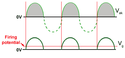
Fig. 6.2.2 SCR Resistive Triggering
The time or phase angle at which the SCR will be triggered can be varied by changing the amplitude of the gate waveform. As can be seen from the animation in Fig. 6.2.2. the smaller the gate signal amplitude, the later the SCR switches on. Changing the amplitude of the trigger waveform therefore controls the switch-on time of the SCR. Note however that as a thyristor is basically a rectifier diode it only conducts during half of the AC cycle, a single SCR can therefore only deliver 50% of the available AC power. Also, in using this very basic form of control, the current flow through the SCR is only controllable over half of the positive half cycle, that is a quarter of the full AC cycle. It can be seen that once the switch-on time reaches the peak amplitude of the AC wave it cannot be adjusted further, as the peak amplitude of the trigger waveform will no longer reach the SCR gate firing potential and so will not trigger the SCR after this point.
Fig. 6.2.3 AC Control Using Resistors

Fig. 6.2.3 Video not available in print format
It can also be seen from both the animation, and the video in Fig 6.2.3, that when using the simple resistive method, control is not very linear; initially the current through the SCR changes only by a relatively small amount, but there is a more rapid change just before conduction ceases. Look carefully at the inset showing the lamp in the video; it only begins to visibly dim just as the switching time is close to the peak value of the AC wave.
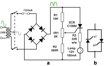
Fig. 6.2.4 Full Wave SCR Control Methods
Full Wave SCR Control
The basic SCR operation described above can be considerably improved with some simple modifications. Perhaps the greatest drawback of the simple resistive control is that the range of adjustment could only cover 25% of the whole AC wave. This is due to the diode action of the SCR only conducting during the positive going half of the AC wave. To allow conduction during the negative going half of the AC wave, the AC can be rectified using a full wave rectifier, as shown in Fig. 6.2.4(a). As both halves of the AC wave will now be positive going, the range of adjustment is now improved to nearly 50%. An alternative is to use a second SCR connected in anti-parallel as shown in Fig. 6.2.4(b) so that one SCR conducts during positive half cycles, and the other SCR during negative half cycles. However this parallel arrangement of SCRs can also be obtained simply by using a single Triac instead of two SCRs.
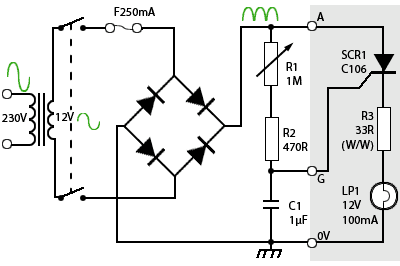
Fig. 6.2.5 SCR Phase Control Demo Circuit
SCR Phase Control
To achieve control over virtually 100% of the AC wave, phase control simply replaces one of the resistors in the resistive control circuit with a capacitor. This now converts the resistor network into a variable low pass filter that will shift the phase of the AC wave applied to the gate. Details of how a low pass filter works can be found here but basically, the values of C and R are chosen so that adjustment of R1 will provide a phase shift from 0° to nearly 90°. To be effective, the variation of R1 needs to give sufficient change in the behaviour of the load device (in this case a 12volt 100mA lamp). As well as shifting the phase of the gate waveform however, the RC filter will also be altering the amplitude of the gate waveform, so the amplitude of the gate waveform also needs to be kept above the firing potential of the SCR type chosen, for switching to take place. From these conditions it can be seen that calculation of suitable values for R and C to provide appropriate control, depend on both phase and amplitude so can get quite complex. Therefore some practical experimentation with R and C values is also most likely to be necessary.
Fig. 6.2.6 SCR Phase Control

Fig. 6.2.6 Video not available in print format
The video in Fig. 6.2.6 shows a working circuit using the component values shown in Fig. 6.2.5. Watching the brightness of the lamp together with the changing waveform shown in the inset image, it can be seen that using phase control does give much improved control over almost the whole 180° of every half cycle, compared to the simple resistive control.
SCR Level Control
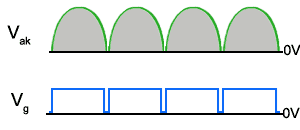
Fig. 6.2.7 SCR Level Control
Another way of switching on the SCR at the appropriate part of the AC cycle is to apply a DC voltage to the gate during the time the SCR is required to conduct. The DC applied to the gate will therefore be a variable width pulse having a voltage level sufficient to cause the SCR to conduct. These pulses must be synchronised with the rectified AC wave so that they always start and end at the correct time relative to the AC waveform.
The animation in Fig. 6.2.7 illustrates the basic method of triggering an SCR using level control. The SCR is triggered (switched on) for a period during each rectified AC half cycle by a voltage Vg applied to the SCR gate. The SCR turns off at the end of each half cycle as the voltage across the SCR falls to near zero, which also coincides with the end of the trigger pulse Vg. The DC pulses may be generated digitally, using a computer output or by using a discrete component circuit such as that shown below in Fig 6.2.8, which uses a 555 timer based monostable. This circuit offers a simple and inexpensive method of demonstrating SCR operation using only low voltages. Two power supplies are used, the shaded area of Fig. 6.2.8 is the AC demonstration power supply described in SCR Module 6.0, which isolates the demonstration circuit from the mains (line) supply. The control section of the circuit must be supplied with a DC voltage of between 5V and 12V. This can be from either a separate DC power supply (e.g. a 'Wall Wart'), a dedicated IC regulated supply, or a battery. The control section of the circuit (black) is also isolated from the AC section (red) by two optocouplers, IC1 and IC3. Because this circuit is already isolated from mains voltage by T1, it would seem unnecessary to use a second method of isolation in IC1, However the main function of IC1 is not isolation in this case, but to act as a zero crossing detector.
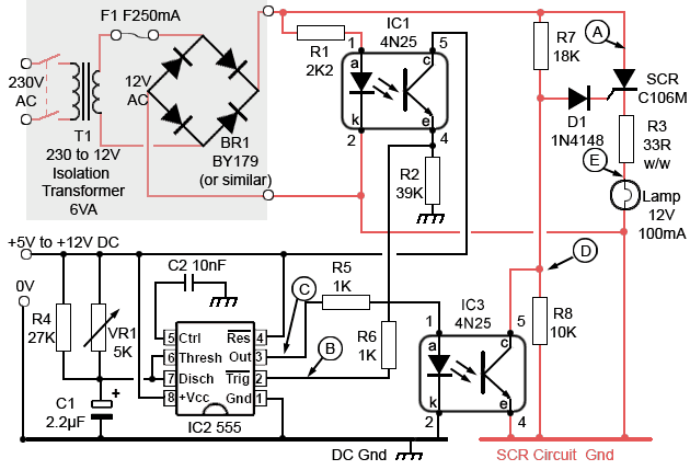
Fig. 6.2.8 SCR Level Triggering Circuit
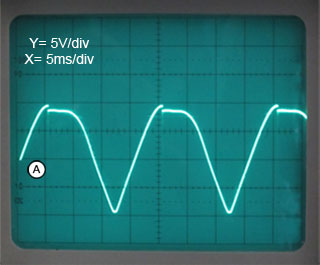
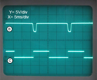
Fig. 6.2.9 SCR Level Triggering Waveforms
Level Triggering Demonstration Circuit
The circuit in Fig. 6.2.8 switches on the SCR at a time chosen by the setting of VR1 during each positive AC half cycle from the low voltage power supply (waveform A). The SCR switches off again as the rectified AC voltage reduces to near zero at the end of each half cycle. The control circuit is based around a 555 timer IC operating in monostable mode, and two 4N25 opto couplers.
As well as isolating the 555 circuitry from the incoming AC, IC1 (4N25) provides a synchronising pulse (waveform B in Fig. 6.2.9). This is achieved by biasing IC1 in common collector mode so that its output transistor conducts for most of the full wave AC input, producing a high (5V) voltage at pin 4, but turns off as the AC wave approaches 0V, producing a 0V output at pin 4 of IC1. These pulses are used to trigger the 555 monostable (IC2) at the start of each half cycle.
Each time IC2 is triggered its output on pin 3 goes high for a time set by the time constant created by variable resistor VR1 and the timing capacitor C1. Notice that VR1 is also connected in parallel with a 27K resistor R4. The purpose of this is to achieve a more accurate time constant than is possible using only the preferred values of VR1 and C1. It would also be possible to fit a preset resistor in place of R4 to obtain the exact duration for the high level trigger pulse produced by IC2.
Fig. 6.2.10 SCR Level Triggering
Fig. 6.2.10 Video not available in print format
Notice that the trigger pulse produced by IC2 (waveform C in Fig. 6.2.9) goes high immediately a synchronising pulse is received, which would turn the SCR on at the start of the half cycle. Also when the trigger pulse returns low this would not switch off the SCR, it would continue to conduct until the end of the half cycle; this is not what is needed. However, waveform C is inverted by the action of the optocoupler IC3, because its output transistor is connected in common emitter mode. Therefore the SCR is triggered during the latter period of the rectified AC half cycle, (waveform D in Fig. 6.2.9). Notice that waveform D does not look like the inverse of waveform C because, as soon as the SCR is triggered the gate input (together with the anode and cathode) follows the shape of the rectified AC wave from the moment of triggering to the time it reaches 0V.
Note that the level triggering circuit described here and shown in operation in the video in Fig. 6.2.10 is not particularly meant to represent a practical circuit for high voltage control, but as a demonstration piece allowing the control of an SCR to be studied. This module therefore provides the opportunity to study SCR triggering modes in more depth, using the low voltage AC power supply described in SCR Module 6.0 and constructing the trigger circuits on breadboard. In practice however, there are some drawbacks to level triggering, which can be overcome by using Pulse Triggering.
SCR Pulse Triggering
Using level triggering as described above has the drawback of creating gate current throughout the 'on' period of the SCR. This creates unnecessary gate current and in high power application can add to heat generated at junction 2 of the SCR, which in turn may reduce long term reliability.
A modification to the circuit shown in Fig. 6.2.8 is illustrated in Fig. 6.2.11. This circuit generates a single narrow pulse (about 4µs in duration) to trigger the SCR at the chosen firing angle, the SCR then continues to conduct until the forward current falls to less than the holding current value at around 0V so greatly reducing the average gate current.
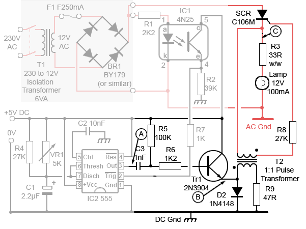
Fig. 6.2.11 SCR Pulse Triggering Circuit
How the Pulse Triggering Circuit Works
The portion of Fig. 6.2.11 shown in pale grey works in the same way as already described for Fig 6.2.8; the output of IC2 (the monostable) consists of variable width positive pulses (waveform A shown in Fig. 6.2.12) where the falling edge of each pulse defines the firing angle of the SCR. (Note that in the level triggering circuit this waveform is inverted before being applied to the gate, so that the falling edge becomes a rising edge to trigger the SCR). In Fig 6.2.11 before the output of IC2 is inverted, it is differentiated by C3 and R5 to produce a series of narrow 4µs positive and negative going pulses corresponding to the rising and falling edges of waveform A. These narrow pulses are fed to the common collector (emitter follower) driver transistor Tr1 via R6. Diode D2 at Tr1 emitter removes the positive going pulses (apart from a small residue due to the forward junction potential of the diode).
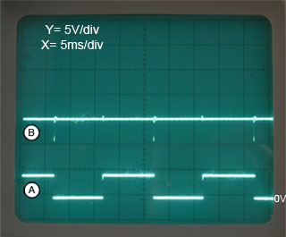
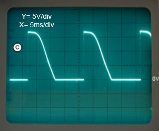
Fig. 6.2.12 SCR Pulse Triggering Waveforms
The negative going pulses (waveform B) at Tr1 emitter are inverted by the 1:1 pulse transformer T2 by connecting T2 secondary in anti-phase to the T2 primary (notice the phase indicator dots next to the primary and secondary windings) so producing positive going trigger pulses for the SCR. T2 also acts as the isolator between the low voltage DC control circuit and the higher voltage AC SCR. Fig. 6.2.12 waveform C shows the SCR cathode waveform, the fast rising edge corresponding to the timing of the trigger pulse delivered to the gate via R8 current limiting resistor; this reduces the current delivered by each trigger pulse to around 100µA.
Both the level triggering and pulse triggering circuits provide reliable triggering and adjustment over nearly the whole 360° of the 50Hz AC wave. Some adjustment of the monostable time constant may be necessary for 60Hz operation. The DC supply voltage level is not critical, between about 5V and 12V.
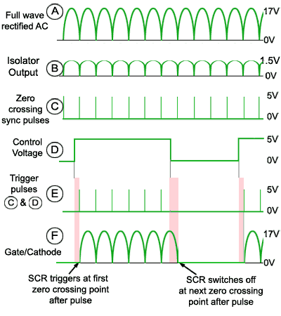
Fig. 6.2.13 SCR Zero Crossing Waveforms
Synchronous (Zero Crossing) Switching
A problem exists however with all the control methods described above. The AC output waveform when the SCR is switched on during each positive half cycle of the AC wave, has a very fast rise time, as the current through the SCR suddenly switches from zero to the instantaneous value of the AC wave. When used with a 230V AC supply this sudden change can be around 325V (the peak value of the AC wave). The waveform may also be a sharp triangular spike if the SCR switches on after the peak value of the wave has occurred. In any case the AC voltage waveform produced by the SCR action will be rich in harmonics, that can generate a serious level of electromagnetic interference (e.m.i.) causing problems not only to other connected circuitry; the interference can also radiate to other nearby electronics as radio frequency interference (r.f.i.) as the harmonics produced can extend well into the radio frequency bands. To avoid these problems alternative control methods may be used. One such method, called 'Synchronous or Zero Crossing Switching' is to only allow thyristors to switch when the mains waveform is at, or very close to zero volts. The thyristor is then switched on for a number of cycles and then switched off again (as the AC voltage passes through 0V) for another number of cycles. The ratio of on to off cycles can then be altered to provide a variation of average power supplied to the load. Fig. 6.2.13 illustrates a theoretical method for achieving zero crossover switching. A practical demonstration circuit is shown in Fig. 6.2.14 and the actual waveforms obtained from the circuit are shown in Fig. 6.2.15.
Waveform A in Fig. 6.2.15 shows the 18Vpp 100Hz waveform applied to the zero crossing circuit from the full wave rectified AC power supply and bridge rectifier (shaded grey in Fig. 6.2.14).
Waveform B is a series of 5V pulses, derived from IC1 optocoupler. As the optocoupler transistor is turned on for most of the positive half cycle of the AC input, this makes the emitter high apart from a narrow pulse as the emitter falls from 5V to 0V each time the AC input falls to 0V. These pulses are therefore synchronised to the zero voltage point of waveform A.
However, as positive going trigger pulses are needed to trigger the SCR, the pulses at B are inverted by Tr1 to create waveform C.
Waveform D is the output of a free running 555 astable oscillator IC2, which produces square pulses at a pulse repetition frequency of about 7Hz and a variable duty cycle adjustable by VR1. This waveform is used to control the ratio of the on and off times of the SCR. As the SCR will be high (on) for a number of 100Hz half cycles, then low (off) for a number of half cycles. The mark to space ratio of the square wave produced by IC2 is adjustable by VR1 to produce an on time of between about 20% and 90% of the periodic time of the astable output. The operation of IC2 is described in more detail in Oscillators Module 4.4.
The outputs of Tr1 (waveform C) and IC2 (waveform D) are applied to the two inputs of the AND gate (IC3). The output of IC3 goes to logic 1 only when both inputs are at logic 1. This produces a series of narrow positive going trigger pulses (waveform E) to trigger the SCR only at the start of those half cycles whilst waveform D is high. The trigger pulses produced are applied to T2, a 1:1 isolating pulse transformer via the emitter follower driver transistor Tr2. The secondary winding of T2 applies the trigger pulses to the gate of the SCR via a current limiter resistor R11 and diode D3. The gate waveform (waveform F) is practically identical to the output waveform at the SCR cathode as there is only a small voltage difference between the gate and cathode of the SCR.
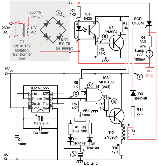
Fig. 6.2.14 SCR Zero Crossing Control Circuit
*Safety Note: Generally 0.25watt resistors are OK for this design, but if the circuit is operated for a prolonged time with no AC supply but with the DC supply still on, there is a possibility that R11 (47R 0.25W) can overheat, as under these conditions it will be passing increased current due to waveform E being a higher current version of the astable output (waveform D). To avoid overheating, R5 could be replaced by a higher wattage version, or preferably both AC and DC supplies should always be turned off when the circuit is not operating!
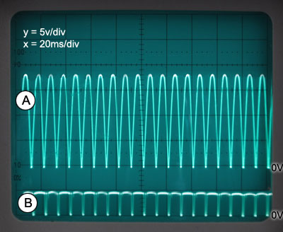
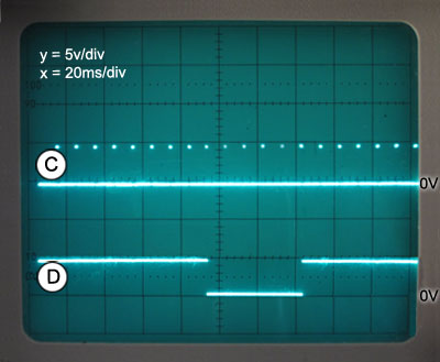
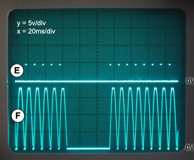
Fig. 6.2.15 Waveforms Fig. 6.2.14 Circuit
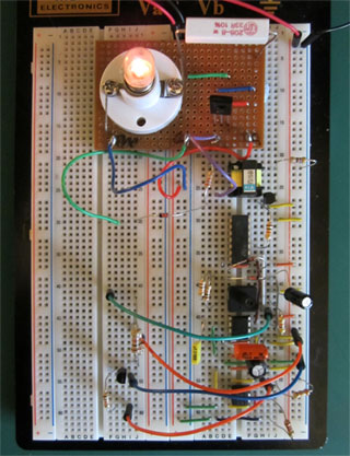
Fig. 6.2.16 SCR Zero Crossing
Breadboard Circuit
SCR Zero Crossing Circuit Operation
This demonstration circuit again uses the low voltage (12VRMS) full wave rectified AC supply described earlier and shaded grey in Fig. 6.2.14.
Fig. 6.2.14. uses two different methods of isolation and demonstrates how the zero crossing control method may be achieved using standard components. It is not meant to represent any particular commercially available solution, nor is it meant to represent the best available method. The purpose of the SCR gate drive circuits discussed in this module is to provide useful demonstrations of commonly used drive techniques and a low voltage environment for relevant experimentation. They can be inexpensively built on standard breadboard or strip board as shown in Fig. 6.2.16 to serve as useful demonstrations, or as student projects. Low voltages are used in these projects to maintain a safer environment, but learnabout-electronics.org does not claim or suggest that any electronic circuit is totally safe, choosing to build and/or use the circuits and methods described on this site is done entirely at your own risk.
The video in Fig 6.2.17 shows the effect of zero crossing control when used to dim a lamp. Notice the pronounced flicker produced as the SCR switches on and off at low frequencies, showing that this solution, whilst removing one problem of SCR control (interference) produces another - the low switching speed and associated flicker. However while this may be a problem for lighting applications, it is not a problem for applications with slowly changing values such as heating control. Zero crossing can therefore be effective in controlling temperature by varying the average power supplied to a heating element. Also, because of the absence of fast changing voltage spikes in zero crossing control, it is more suited to use with inductive loads than drive circuits that switch during the AC cycle.
Fig. 6.2.17 SCR Zero Crossing Control

Fig. 6.2.17 Video not available
in print format