Module 1.4
Amplifier Bandwidth
- After studying this section, you should be able to:
- Describe factors affecting bandwidth in single stage common emitter amplifiers.
- • Stray capacitance and inductance in circuits and components.
- • Gain bandwidth product, cut off frequency fT.
- Describe basic methods for controlling bandwidth
- • in AF amplifiers.
- in RF amplifiers.
Controlling Bandwidth
Any amplifier should ideally have a bandwidth suited to the range of frequencies it is intended to amplify, too narrow a bandwidth will result in the loss of some signal frequencies, too wide a bandwidth will allow the introduction of unwanted signals, in the case of an audio amplifier for example these would include low frequency hum and perhaps mechanical noise, and at high frequencies, audible hiss.
AC Components in a Common Emitter Amplifier
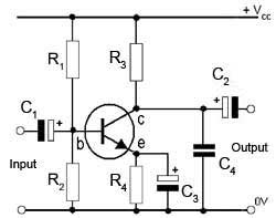
The class A common emitter amplifier circuit shown in Fig 1.4.1 has the DC bias components discussed in Module 1.3 with the AC components (capacitors C1 to C4) added that are necessary for use with an AC signal and also to achieve control over both gain and bandwidth.

Fig. 1.4.1 Class A common emitter amplifier.
The signal must pass through the input and output coupling capacitors C1 and C2 as it passes from input to output. The primary function of these capacitors is to provide DC isolation from voltages in preceding and following circuits. Also however, because the action of capacitors is frequency dependent they also can have an effect on the bandwidth of the amplifier.
C1, together with R1, R2 and the input resistance of the transistor forms a high pass filter, and C1 will normally have a quite large value of capacitance, making the corner frequency of the filter very low. At frequencies below this point however, amplifier gain will be reduced.
C2 will act in a similar manner with the input impedance of any following circuit, also contributing a fall off in gain at low frequencies.
Emitter Decoupling
The emitter decoupling capacitor C3, connected across the emitter stabilising resistor R4 is intended to prevent any AC signal appearing on the emitter, which would otherwise act as negative feedback, severely reducing the gain of the amplifier. The relatively large value of C3 almost entirely removes any AC from the emitter, but it will have some reactance at the lowest frequencies and so allow some very low frequency signals to appear on the emitter, (assuming that these frequencies have not been removed by the action of C1 and C2 as described above) and whilst C3 contributes to higher gain over most of the bandwidth, gain at very low frequencies may not be improved.
The values of C1, C2 and C3 are therefore chosen to give the required fall off in gain at the low frequency end of the bandwidth.

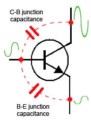
Fig. 1.4.2 Junction Capacitance.
High Frequency Effects
At high frequencies the amplifier gain tends to be reduced to some extent by the presence of small amounts of inductive reactance (which increases with frequency) within the circuit wiring and components, but mainly by stray capacitances. These are not necessarily recognisable capacitor components but may be unavoidable capacitance effects within the circuit wiring and the components themselves.
Both CMOS and bipolar transistors possess capacitance in their junctions. As shown in Fig 1.4.2, the base-collector and base-emitter junctions of a bipolar transistor actually form very small capacitors due to the (insulating) depletion layers on either side of the base. At very high frequencies, normally in the hundreds of MHz, these tiny ´capacitors´ will form negative feedback paths by feeding anti phase signals between the collector and base, and in phase signals across the base-emitter junction.
Each transistor therefore has a limit to its high frequency current gain, and this is normally listed in transistor data sheets as the cut-off frequency fT. This is the frequency at which the small signal current gain hfe falls to 1. As gain begins to fall off at 6dB per octave (a doubling in frequency) well before fT is reached, the transistor needs to be operated at frequencies considerably lower than fT. Because of the relationship between frequency and gain in transistors, fT is also commonly listed as "Gain Bandwidth Product".
Stray capacitance between closely packed wiring and components can also reduce gain at high frequencies, as well as causing other problems such as instability and oscillation, so the practical upper limit of operation for an amplifier is affected by a number of causes. In many practical amplifier circuits however, these extreme high frequency limits would not be approached; there is no point in designing an amplifier that has appreciable gain at frequencies higher than the highest signal frequency required. To do so would mean that in this region the amplifier would be amplifying mainly high frequency noise (e.g. hiss in the case of an audio amplifier.
Audio Harmonics
However restricting high frequency about 20kHz (the theoretical limit of human hearing)assumes that the signals to be amplified are pure sine waves; In practice there is a trade off between a bandwidth wide enough to handle all the signals required, and a high frequency limit low enough to limit unwanted noise.
Most audio signals will be complex waves of many different and ever changing shapes. Audio signals are complex AC waves having fundamental frequencies in the range of 20Hz to 20kHz but also many higher frequency harmonics. To preserve the original shape of the signals (i.e. not introduce distortion) it is important that at least some of these harmonics are preserved. Therefore it is not advisable to sharply cut off the high frequencies at an arbitrary 20kHz, but rather allow some amplification of the apparently inaudible harmonic frequencies, which will contribute to the complex shape of the audible waves, especially where these signals contain sudden changes (fast transients) that require the presence of high frequency components to maintain their wave shape.

Fig. 1.4.3 Shaping the Audio Response Curve.
There are several ways to ensure that the high frequency cut-off occurs at an appropriate frequency, reducing noise and instability but keeping the important harmonics in an audio amplifier. One such way is in a multi stage amplifier is to use a low pass filter in one of the amplifier stages. In Fig. 1.4.1 for example, C4 is effectively acting in conjunction with R3 as a low pass filter, (remember that as far as AC signals are concerned, the top end of R3, connected to the positive supply (+Vcc) is the same point as ground) preventing amplification of unwanted high frequencies. Its effect is to limit HF gain as shown in Fig. 1.4.3.
Tuned RF Amplifiers
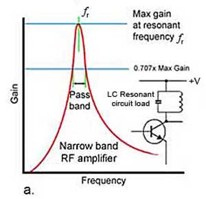
In circuits designed to amplify radio frequency (RF) signals, the load resistor is replaced by either a LC parallel resonant circuit (Fig. 1.4.4a) or some form of ceramic or crystal filter. The design of these filters, or the values of L and C are such that the load circuit resonates and effectively becomes a high resistance at the centre of the amplified frequency band. This can give a frequency response curve that that is sharply peaked over a narrow band of frequencies, called the pass band, frequencies above and below this band being rejected.
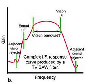
In modern designs, the use of ceramic filters and surface acoustic wave (SAW) filters allows designs with quite complex frequency response curves (Fig. 1.4.4b) that do not (as with LC circuits) require manual adjustment. They are commonly used in systems such as cell phones, and also in analogue TV receivers where both sound and vision signals at different frequencies are amplified by different amounts in the same amplifier. The amplifier response is also designed to have low gain at specific frequencies to reject signals of other transmissions on adjacent channels.


