Google Ads
Module 10.2
Practical Parallel Circuits
- After studying this section, you should be able to:
- • Describe the action of practical LCR parallel circuits with the use of phasor diagrams .
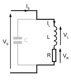
Fig. 10.2.1a
Fig 10.2.1a Looking at the inductive (LR) branch of the parallel circuit.
Fig 10.2.1a shows a practical LCR parallel circuit, where R is the internal resistance of the inductor L, plus any additional resistance in the inductive arm of the circuit. Before considering the whole circuit, the inductive branch will be examined as though it was a separate LR series circuit, and the arm containing C will be temporarily ignored. An understanding of what happens in L and R will be the foundation for a better understanding of the whole circuit.
Fig 10.2.1b Phasors for the L and R
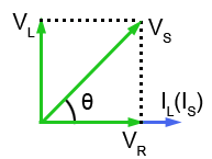
Fig. 10.2.1b
Fig 10.2.1b shows a phasor diagram for the LR branch of the circuit in Fig 10.2.1a, drawn as it would be for an LR series circuit. The branch of the circuit containing C is being ignored. The reference phasor is (IS) and because the same current (IS) passes through both R and L, the phasors for IL and VR will be in the same phase. VS is the phasor sum of VL and VR.
In a parallel circuit it will be the supply voltage VS that is common to all components and so will be used as the reference phasor in Fig 10.2.2.
Fig 10.2.2 Phasors for the LR branch of a parallel LCR circuit
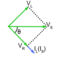
Fig. 10.2.2
Fig 10.2.2 shows Fig 10.2.1b modified for a parallel circuit. The complete diagram is rotated so that the phasor for VS is horizontal and used as the reference phasor. This is because, when describing PARALLEL circuits, it is the supply voltage (VS) that is common to all components.
The phasors for IL and VR are in phase with each other, and VL leads IL by 90°. However the phase angle θ between VS and IL (and IS) will vary with frequency. This is because the value of XL and therefore VL will increase as frequency increases. Because VL changes in length, and VS is fixed, angle θ will change, which will have an effect on the phasor diagrams for the complete LCR circuit.
Fig 10.2.3a Phasors for the LR branch of a parallel LCR circuit at HIGH frequency.
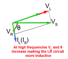
Fig. 10.2.3a
Fig 10.2.3a represents the condition when the frequency of the supply is high, so XL and therefore VL will be large. VS is the phasor sum of VR and VL.
It follows then, that the phase angle θ is some value between 0° and 90° with IL lagging on VS. In the ideal circuit IL always lags on VS by 90°, so the effect of adding some resistance will be to reduce the angle of lag (θ). At higher frequencies however VL and θ increase and the circuit becomes more like a pure inductor.
It is important to note that the value of XL depends on both the frequency and the value of inductance. The value of R will also depend on the design of the inductor and so VL and θ will depend on both the frequency of VS and on component values.
Fig 10.2.3b Phasors for the LR branch of a parallel LCR circuit at LOW frequency.
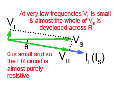
Fig. 10.2.3b
Fig 10.2.3b shows the effect of reducing the frequency of VS to a low value. XL will now be smaller, and so will VL.
VS is still the phasor sum of VR and VL, due to the reduction in XL, IL will increase and most of the supply voltage will be developed across R, increasing VR. With VL reduced in amplitude and VR increased, angle θ is very small making IS and VS nearly in phase, making the circuit much more resistive than inductive.
This means that in a practical circuit, where the inductor must possess some resistance, the angle θ by which IL lags VS is not the 90° difference that would be expected of a pure inductor, but will be somewhere between 0° and 90°, depending on the frequency of the supply. At frequencies where XL is much greater than R the circuit is predominantly inductive but at comparatively low frequencies where the normally small value of R may become comparable or even greater than XL the circuit becomes more predominantly resistive.
Fig 10.2.4a The complete LCR parallel circuit.
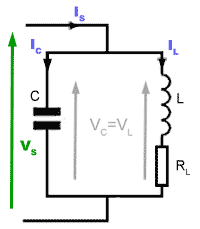
Fig. 10.2.4a
Returning to the whole LCR circuit, three phasors, IC, IL and the reference phasor VS are used to show the operation of the complete parallel circuit shown in Fig 10.2.4a.
Current phasors for L and C are used because VL (combined with its internal resistance RL) and VC will be the same as they are connected in parallel across the supply. It is the currents through L and through C that will differ. The phasor for IC leads VS (which is also the voltage across C and L) by 90° and IL lags VS by somewhere between 0°and 90°, depending on component values and supply frequency.
Fig 10.2.4b Phasors for the complete LCR parallel circuit.
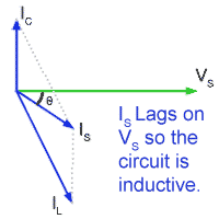
Fig. 10.2.4b
In Fig 10.2.4b a fourth phasor IS (the supply current) will be the phasor sum of IC and IL, which in this diagram is larger than IC. The two current phasors IC and IL are not in exact anti phase so the phasor for IS is lagging that for VS. Therefore the circuit is inductive.


